Method for utilizing heavily doped silicon feedstock to produce substrates for photovoltaic applications by dopant compensation during crystal growth

a technology of dopant compensation and crystal growth, which is applied in the direction of crystal growth process, polycrystalline material growth, chemistry apparatus and processes, etc., can solve the problems of high cost of purifying silicon, insufficient effect of reducing dopant atoms to an acceptable level, and high cost of purification silicon. achieve good solar cell performance, high resistivity, and respectable efficiency

Inactive Publication Date: 2008-09-11
SOLAR POWER INDS
View PDF8 Cites 25 Cited by
  • Summary
  • Abstract
  • Description
  • Claims
  • Application Information

AI Technical Summary

Benefits of technology

[0021]It is noted that since compensated silicon involves (nearly) balancing the concentration of one dopant type against the opposite type, there is a practical limit to how closely this balancing can be achieved. A net doping concentration that is 10% of the majority doping concentration is possible. Obtaining a net doping that is 1% of the majority doping may be achieved only with difficulty.
[0022]As supported by the theoretical expectations for lifetime and diffusion constant in compensated silicon described above, good solar cell performance can be obtained using silicon feedstock containing multiple dopant impurities. For example, in accordance with the present invention, silicon ingots may be prepared with aluminum levels in the range 0.04-0.10 ppma, boron levels in the range 0.5-2.5 ppma, and phosphorus levels in the range 0.2-2.0 ppma as determined by mass spectroscopy (R. K. Dawless, R. L. Troup, and D. L. Meier, “Production of Extreme-Purity Aluminum and Silicon by Fractional Crystallization Processing,” Journal of Crystal Grow...

Problems solved by technology

This high cost is not due to the unavailability of silicon, since silicon is the second most abundant element in the earth's crust, behind only oxygen.
Rather, it is due to the high cost of purifying silicon to a level required for semiconductor applications, including P...

Method used


Image

  • Method for utilizing heavily doped silicon feedstock to produce substrates for photovoltaic applications by dopant compensation during crystal growth
  • Method for utilizing heavily doped silicon feedstock to produce substrates for photovoltaic applications by dopant compensation during crystal growth
  • Method for utilizing heavily doped silicon feedstock to produce substrates for photovoltaic applications by dopant compensation during crystal growth

Examples


example 1

Y BOOST FROM DOPANT COMPENSATION

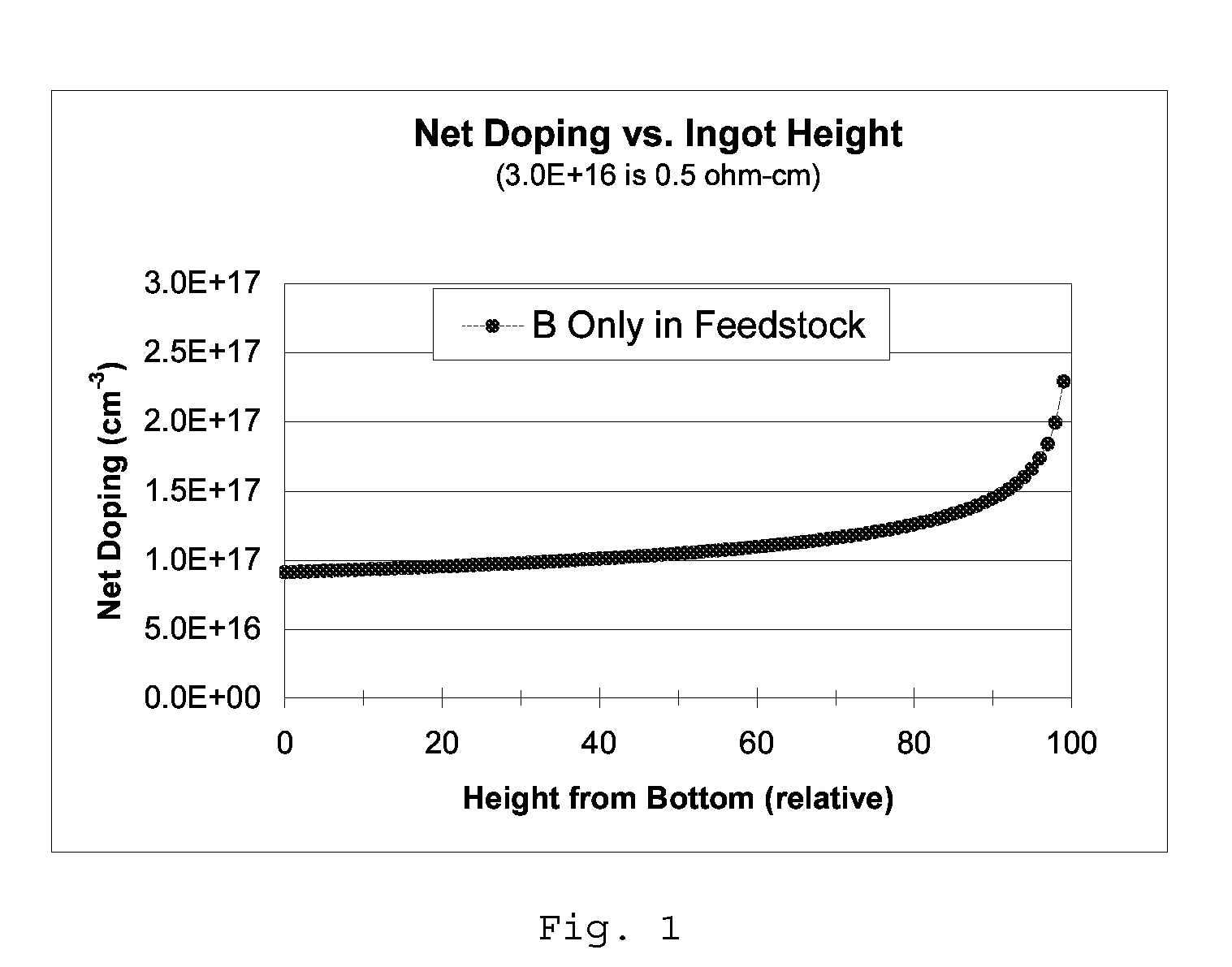
[0050]A candidate silicon feedstock, identified as “Brand A-6N,” was procured. A GDMS analysis indicated a very high concentration of boron and phosphorus, with boron at 4.6 ppmw (12.0 ppma or 6.0×1017 cm−3) and phosphorus at 15 ppmw (13.6 ppma or 6.8×1017 cm−3). Note that the boron concentration in the feedstock is 20 times the maximum value desired in the silicon crystal (3.0×1016 cm−3). Troublesome metals were generally below their respective GDMS detection limits, with V below 0.005 ppmw, Li, Ti, Mn, Co, Ni, Ag, and W all below 0.01 ppmw, S, Cu, Zn, Ga, As, Mo, Sb, and Pb all below 0.05 ppmw, and Cr below 0.1 ppmw. Only Fe and Al were detected at 0.06 ppmw and at 0.32 ppmw, respectively. A full-sized ingot (ID 060206-2), with a mass of 265 kg, was produced at Solar Power Industries in a DSS (directional solidification of silicon) furnace using 225 kg of the Brand A-6N feedstock and 40 kg of undoped silicon. FIG. 5 depicts the expected net doping i...

example 2

ION OF MARKET-WORTHY CELL PERFORMANCE WITH INITIAL DOPANT COMPENSATION

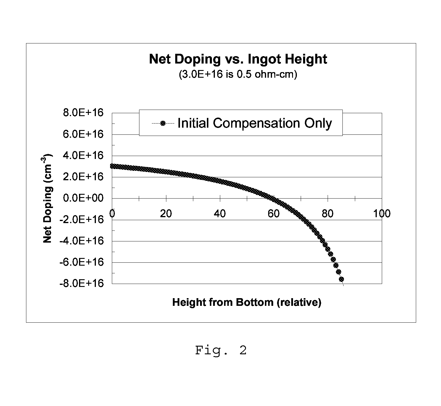
[0054]In order to demonstrate the benefits of dopant compensation in a controlled manner, a full-sized (265 kg) silicon ingot was produced using intrinsic silicon with boron added at a concentration of 0.5 ppmw (6.5×10¹⁶ B / cm3). This represented silicon feedstock which had a residual boron content at a level which may be obtained by some low-cost purification processes. With a segregation coefficient of 0.80, the expected boron concentration at the beginning (bottom) of a directionally-solidified ingot is 5.2×10¹⁶ B / cm3. This is almost twice the maximum level of 3.0×10¹⁶ B / cm3 desired in a substrate for solar cells, and which would increase as the crystal grows as the melt becomes more highly concentrated in boron. To bring the net doping concentration into the desired range for this simulated impure feedstock, the excess boron was compensated with arsenic in the initial silicon charge. The purpose was to demonstr...

example 3

DOPING CONCENTRATION IN THE MELT AND SAMPLING THE MELT

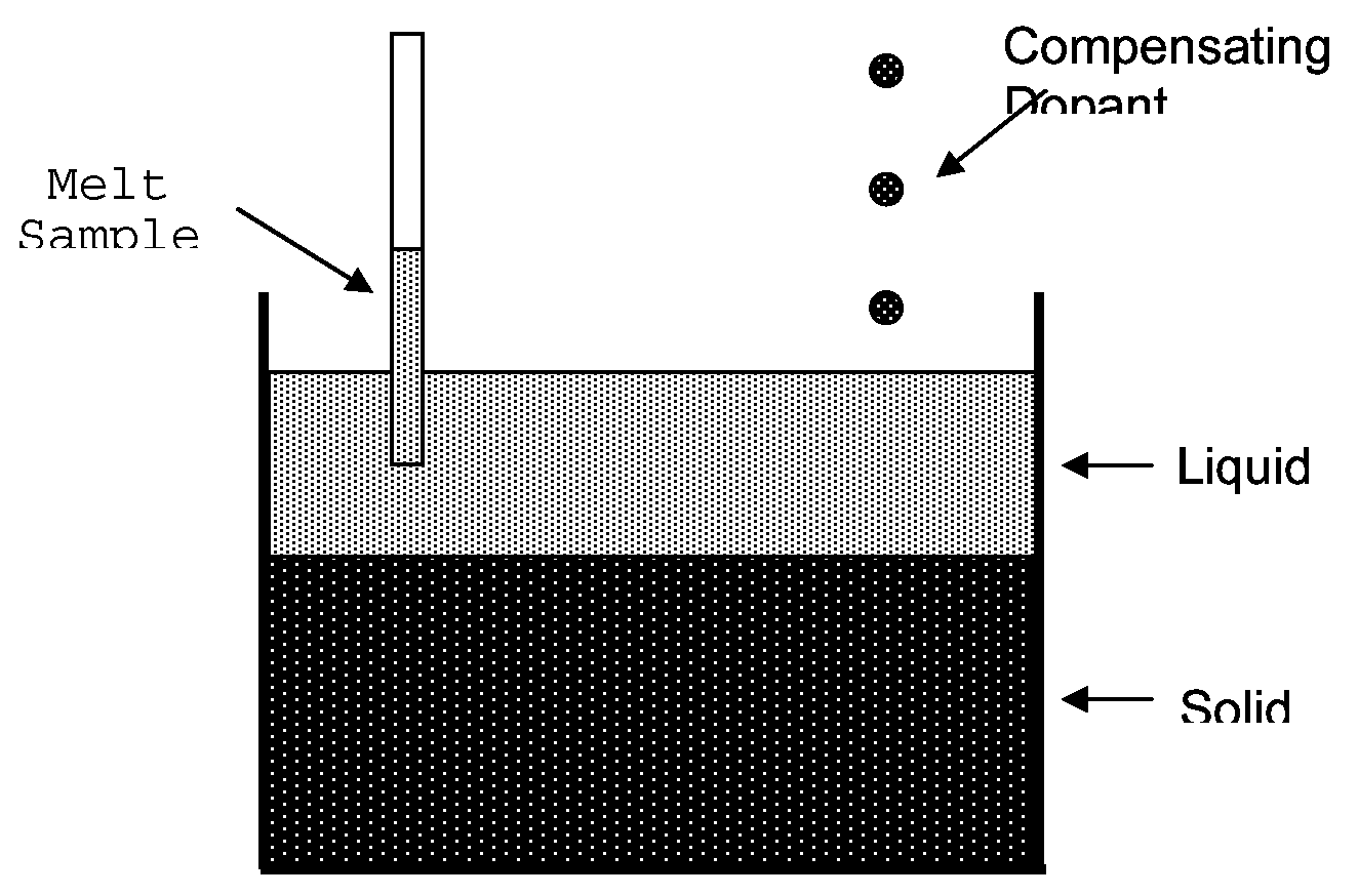
[0061]Dendritic web silicon ribbon crystals were grown in Run SPI-101-5. The dendritic web crystal growth technique was different from the directional solidification technique employed in the above Examples in that crystals are grown at atmospheric pressure rather than at reduced pressure, the melt volume was much smaller at 0.3 kg rather than 265 kg, crystals were single crystal ribbon that exit the growth chamber rather than a multicrystalline ingot which remained inside the growth chamber, and melt volume remained approximately constant during a crystal growth run rather than decreasing during the run. It is also noted that operation at atmospheric pressure facilitated adding dopant to the melt and also sampling the melt.

[0062]The dendritic web growth run started with a 335 g melt to which 2.3×10¹⁹ boron atoms were added via silicon doped with boron to 0.0045 Ω-cm. The dendritic web crystal grown from this melt was measured to...


PUM


Abstract

A method for using relatively low-cost silicon with low metal impurity concentration by adding a measured amount of dopant before and/or during silicon crystal growth so as to nearly balance, or compensate, the p-type and n-type dopants in the crystal, thereby controlling the net doping concentration within an acceptable range for manufacturing high efficiency solar cells.

Description

BACKGROUND OF THE INVENTION[0001]1. Field of the Invention[0002]This invention relates to the manufacture of photovoltaic solar cells. More particularly, this invention relates to methods for utilizing heavily doped silicon feedstock to produce substrates for photovoltaic applications by dopant compensation during crystal growth.[0003]2. Description of the Background Art[0004]Photovoltaic (PV) devices for producing electrical energy directly from sunlight have become increasingly popular in recent years. Worldwide production of PV cells in 2005 exceeded 1,500 MW, with power output determined under standard test conditions (1 kW / m2 light intensity, Air Mass 1.5 Global spectrum, and cell at 25° C.). With these solar cells typically encased in a module having a selling price of approximately $5 / W, the 1,500 MW production represents a $7.5 B / year industry. Furthermore, the worldwide industry output, measured in MW / year, has a compounded annual growth rate in excess of 30%. Silicon solar...

Claims


Application Information

Patent Timeline
IPC IPC(8): H01L21/00
CPCC30B11/04C30B15/007H01L21/228C30B29/06C30B15/04
Inventor BUCHER, CHARLES E.MEIER, DANIEL L.
Owner SOLAR POWER INDS
Why Eureka
Try Eureka