
Saw devices, processes for making them, and methods of use

Active Publication Date: 2008-09-25
GEORGE WASHINGTON UNIVERSITY
View PDF68 Cites 45 Cited by
  • Summary
  • Abstract
  • Description
  • Claims
  • Application Information

AI Technical Summary

Benefits of technology

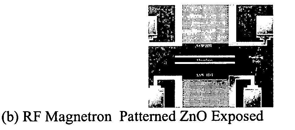
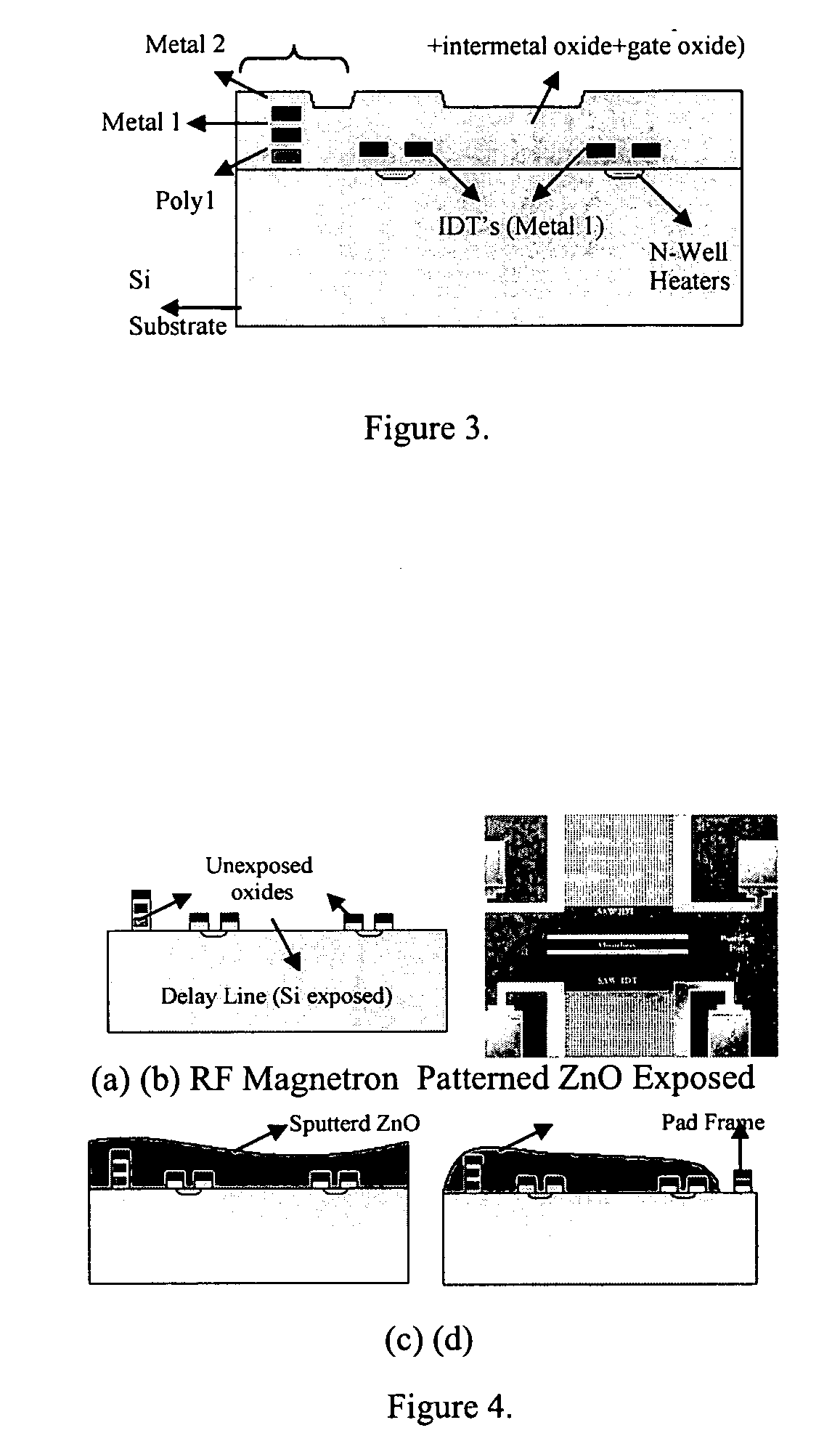
[0019]A heat control structure built within the substrate silicon during the CMOS process is also part of the inventive subject matter and can be adopted in any of the CMOS chip devices herein. In preferred embodiments, the heat control structure is an n-well layer that has a TCR of 0.5-0.75% / K, which is the highest among various CMOS process layers and wherein the n-well provides an embedded heater structure that can directly control the temperature of the substrate and the mass sensitive area without causing any disturbance on the SAW delay line path or the IDT finger design.
[0026]Another preferred embodiment of the invention includes a SAW device made by the processes described herein, especially those wherein signal control and processing circuitry are integrated on the same chip, and those wherein the n-well layer has a TCR of 0.5-0.75% / K, which is the highest among various CMOS process layers and wherein the n-well provides an embedded heater structure that can directly control the temperature of the substrate and the mass sensitive area without causing any disturbance on the SAW delay line path or the IDT finger design.
[0029]It is believed that advantages of the exemplary embodiments and / or exemplary methods of the present invention may include optimized biosensor devices, improved biosensor arrangement performance, determination of effective sensing media immobilization approaches, and SAW based biosensors that may be used to provide continuous, in-situ, and rapid detection and quantification of analytes in samples.

Problems solved by technology

Such sensors may, however, have various weaknesses, such as, for example, low sensitivity, selectivity, or an inability to be hybridized or integrated into sensing chip technology.
Such materials may, however, have varying transverse acoustic wave velocities, low electromechanical coupling coefficients, non-linear temperature coefficients, and may react chemically with the environment.
Previously, creation of SAW devices has been complicated and, in the case of CMOS fabrication, it has been unworkable as the chip would be destroyed by the temperatures required to integrate the SAW device.

Method used


Image

  • Saw devices, processes for making them, and methods of use
  • Saw devices, processes for making them, and methods of use
  • Saw devices, processes for making them, and methods of use

Examples


examples

[0113]In these example implementations, one deposition step is eliminated since standard CMOS metal layers are used to implement the transducers' structures. The maturity and precision of the standard 0.6 μm CMOS technology enables us to manufacture very well-defined metal features to implement the transducers, with minimum widths of 0.9 μm, resulting in very high frequency resonators of 1.02 GHz.

[0114]These examples present the design, fabrication, equivalent circuit model and characterization measurements of three two-port resonators. The design of the CMOS SAW resonators is described first, where the key design factors that affect the resonant frequency and quality factor are highlighted. Next, the fabrication sequence of implementing the surface acoustic wave resonators in CMOS with three additional post-processing steps is illustrated in detail. Characterization of the piezoelectric zinc oxide layer using x-ray diffraction, scanning electron microscopy (SEM) and atomic force mi...

example

V. Experimental Measurements and Discussion

[0137]The designed chip consisting of three resonators is shown in FIG. 17. To obtain S21 and S11 measurements, each resonator was probed using two coplanar G-S-G probes in the Cascade Microtech 9500 Parametric Probe Station connected to the HP8712 network analyzer. The coplanar probes were connected to the network analyzer using cables, SMA and N connectors. The experimental setup is shown in FIG. 18.

[0138]A Thru calibration structure was also included in the design to improve measurement accuracy. Both metal 2 and metal 1 in CMOS was used to implement the Thru structure. To avoid the probes crashing and damaging one another, the distance between the two probes was set to be 200 μm [19].

A. Analysis of Measurement Results

[0139]The S21 measurements provide the insertion loss (IL), series resonant frequency (fs) and parallel resonant frequency (fp). The S21 transmission magnitude and phase measurements as well as the S11 reflection measuremen...


PUM

PropertyMeasurementUnit
Lengthaaaaaaaaaa
Lengthaaaaaaaaaa
Lengthaaaaaaaaaa

Abstract

The design, fabrication, post-processing and characterization of a novel SAW (Surface Acoustic Wave) based bio / chemical sensor in CMOS technology is introduced. The sensors are designed in AMI 1.5 μm 2 metal, 2 poly process. A unique maskless post processing sequence is designed and completed. The three post-processing steps are fully compatible with any CMOS technology. This allows any signal control / processing circuitry to be easily integrated on the same chip. ZnO is used as the piezoelectric material for the SAW generation. A thorough characterization and patterning optimization of the sputtered ZnO was carried out. The major novelties that are introduced in the SAW delay line features are: The embedded heater elements for temperature control, compensation and acoustic absorbers that are designed to eliminate edge reflections and minimize triple transit interference. Both of these attributes are designed by using the CMOS layers without disturbing the SAW performance.

Description

PRIORITY[0001]This application claims priority under 119(e) to U.S. 60 / 793,328 filed 20 Apr. 2006.GOVERNMENT INTEREST[0002]This was supported in part by NSF under Grant 0225431.BACKGROUND[0003]1. Field of the Invention[0004]The present invention relates to the field of surface acoustic wave (SAW) devices, and specifically to improvements to in their manufacturing which then provides additional applications for use.[0005]2. Description of the Prior Art[0006]Acoustic wave sensors use a detection arrangement that is based on perturbations to mechanical or acoustic waves. As an acoustic wave propagates through or on the surface of the acoustive wave sensor material, any changes to the physical or chemical characteristics of the wave path may affect the velocity and / or amplitude of the acoustic wave. These changes may be correlated to the corresponding physical, chemical, or biological quantities being measured to provide sensing.[0007]There may be various biological and chemical sensors...

Claims


Application Information

Patent Timeline
IPC IPC(8): G01N21/75H01L41/22H01L41/04
CPCG01N29/022G01N29/2462G01N29/326G01N2021/1729Y10T29/42G01N2291/0256G01N2291/0423H03H3/08H03H9/42G01N2291/0255
Inventor ZAGHLOUL, MONATIGLI, ONUR
Owner GEORGE WASHINGTON UNIVERSITY
Learn More