Clad textured metal substrate for forming epitaxial thin film thereon and method for manufacturing the same
a technology of textured metal substrate and epitaxial layer, which is applied in the direction of transportation and packaging, superconductor devices, vacuum evaporation coating, etc., can solve problems such as harm, and achieve the effect of high quality and high strength
- Summary
- Abstract
- Description
- Claims
- Application Information
AI Technical Summary
Benefits of technology
Problems solved by technology
Method used
Image
Examples
exemplary embodiment 1
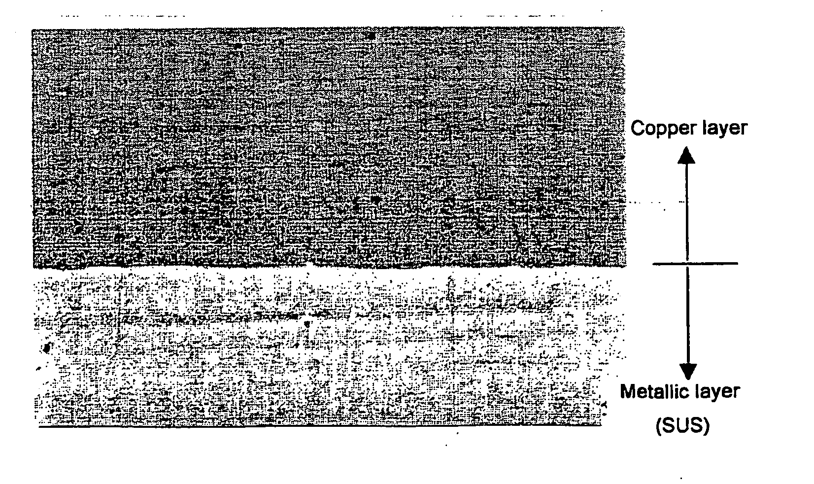
[0042]A tape-shaped copper sheet with a thickness of 3,000 μm was prepared and was cold-rolled (at room temperature) with a reduction roll at a working rate set at 95%. At this time, the copper sheet was electrolytically polished and then finish-rolled by using a lapping roll made from cemented carbide. The copper sheet was electrolytically polished in a sulfuric-acid-based electrolytic solution at a current density of 35 A / dm2 for 30 seconds. After rolled, the copper sheet was heat-treated and the crystal structure was oriented. In the heat treatment step, the copper sheet was heated in an atmosphere containing 95% of nitrogen gas and 5% of hydrogen gas at 700° C. for 30 minutes.
[0043]Next, a metal sheet to be cladded with the above described copper sheet was prepared. The prepared metal sheet was a stainless steel sheet (SUS304) which had been rolled into a tape shape with a thickness of 100 μm beforehand.
[0044]Then, the copper sheet and the metal sheet were cladded by a surface a...
exemplary embodiment 2
[0053]A clad textured metal substrate was manufactured by heat-treating the same copper sheet as in Exemplary embodiment 1 at a changed temperature of 200° C. so as to orient the structure of the surface, and on the same conditions as in Exemplary embodiment 1 except the heat treatment temperature.
exemplary embodiment 3
[0057]Here, a clad textured metal substrate having an intermediate layer was manufactured and the usability was examined. At first, a clad substrate manufactured in Exemplary embodiment 1 was plated with nickel. At this time, a nickel layer was formed into the thickness of 1 μm (Sample 1) on plating conditions of a current density in a range of 1 to 10 A / dm2 and a bath temperature in a range of 40 to 60° C. In addition, substrates having an intermediate layer made from various materials described below on the nickel layer were prepared.
TABLE 1Thickness of intermediate layerSubstrate structure(total)Sample 1Cu / Ni 1 μmSample 2Cu / Ni / YSZ / CeO21.5 μmSample 3Cu / Ni / MgO / CeO21.3 μmSample 4Cu / Ni / CeO2 / YSZ / CeO21.8 μmSample 5Cu / Ni / STO / Y2O31.6 μmCu is a metallic layer of an underlayer.
[0058]The intermediate layer (YSZ, cerium oxide or the like) was formed on nickel by using a PLD method. A target having the same composition as in the objective thin film was used. A substrate temperature was set a...
PUM
| Property | Measurement | Unit |
|---|---|---|
| Fraction | aaaaa | aaaaa |
| Thickness | aaaaa | aaaaa |
| Thickness | aaaaa | aaaaa |
Abstract
Description
Claims
Application Information


