Process For Manufacturing A Gallium Rich Gallium Nitride Film

a gallium nitride and gallium rich technology, applied in the direction of crystal growth process, polycrystalline material growth, after-treatment details, etc., can solve the problems of reduced detection formation, limited cost effective application of present devices, and high cost of sapphire or silicon carbide substrates, etc., to achieve increased conductivity and/or crystallinity

Inactive Publication Date: 2008-11-20
BUTCHER KENNETH SCOTT ALEXANDER +2
View PDF6 Cites 83 Cited by
  • Summary
  • Abstract
  • Description
  • Claims
  • Application Information

AI Technical Summary

Benefits of technology

[0013]annealing the gallium nitride at a temperature and time sufficient to increase the conductivity of the gallium nitride.
[0071](c) means for annealing the said film at a temperature of from about 20° C. to about 700° C. for a time sufficient to decrease the resistivity of the gallium rich gallium nitride film to below 1000 ohm cm.

Problems solved by technology

Although GaN made using the aforementioned conventional processes includes a large number of defects, it is normally considered single crystal material.
However, substrates made of sapphire or silicon carbide tend to be expensive so that the cost effective application of present devices is limited.
Requirements for greater reduction in detect formation require more sophisticated, more expensive techniques, such as ELOG, be applied.
Growth at high temperatures also entails a large expenditure in temperature resistant growth equipment and ancillaries.
However, it is well known that GaN material grown at such low growth temperatures is of lower quality because polycrystalline material is prevalent.
One of the disadvantages of the aforementioned process for the production of gallium nitride above 950° C. is that the process temperature required is high, which results in high energy losses and which requires the use of special materials.
Another disadvantage is that the substrates used at these high temperatures are not ideally matched to GaN.

Method used


Image

  • Process For Manufacturing A Gallium Rich Gallium Nitride Film
  • Process For Manufacturing A Gallium Rich Gallium Nitride Film
  • Process For Manufacturing A Gallium Rich Gallium Nitride Film

Examples


example 1

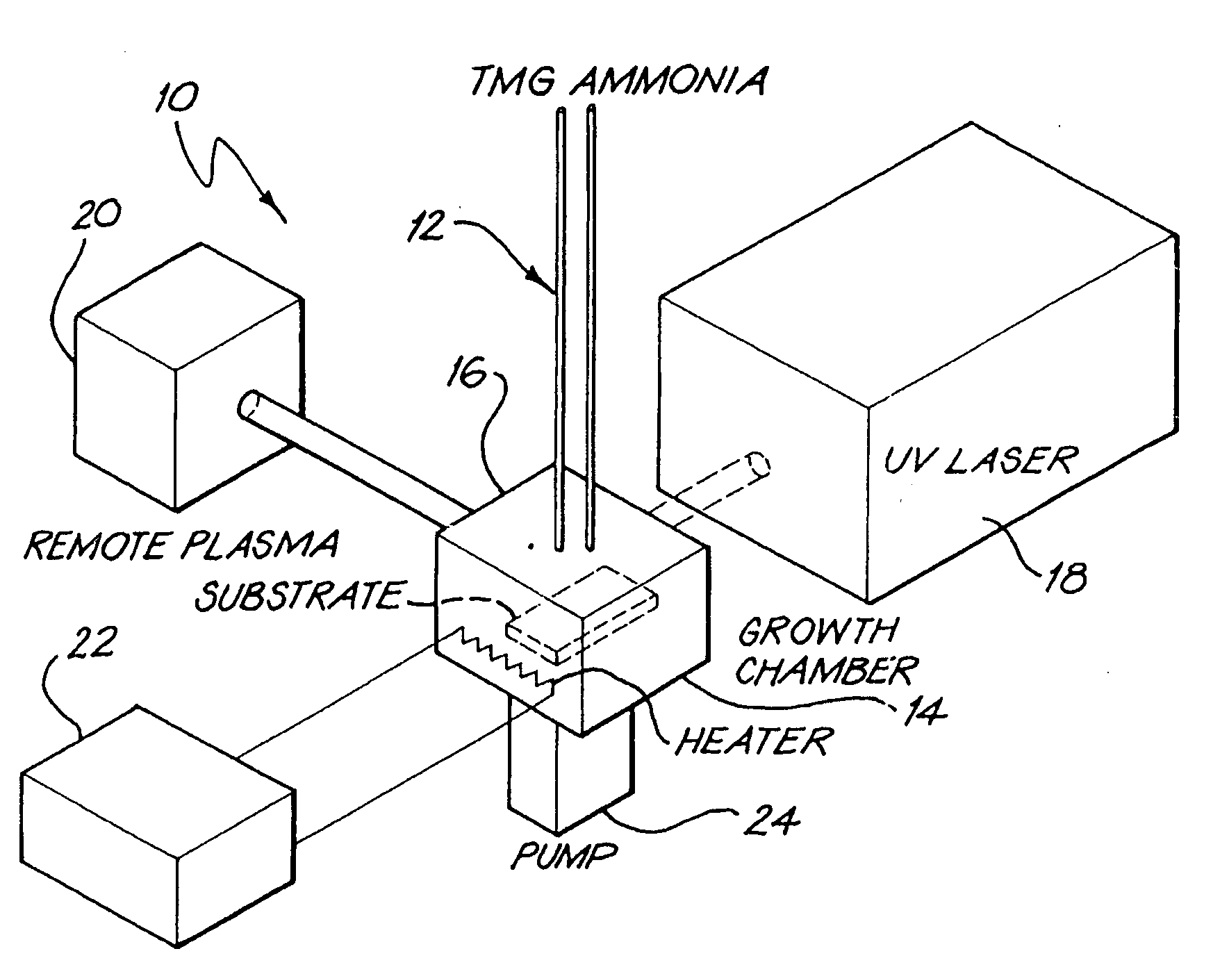
[0113]Fifteen films of gallium nitride (GaN) were grown at 540° C. on (1,0,0) silicon, using a remote plasma enhanced laser induced chemical vapour deposition (RPE-LICVD) technique. The quality of films grown using the aforementioned technique may be comparable to MBE grown material with unintentionally doped n-type material being produced with room temperature mobilities as high as 100-200 cm2 / V·s. [1].

[0114]A high vacuum system was used for the film growth, and the oxygen content of the films was moderated by controlling the background pressure prior to growth. From 1×10⁻⁴ Torr, to 2×10⁻⁶ Torr dependent on the condition of the chamber at the time of growth.

[0115]The samples were all grown under similar conditions-apart from the variation in the background vacuum level as mentioned before.

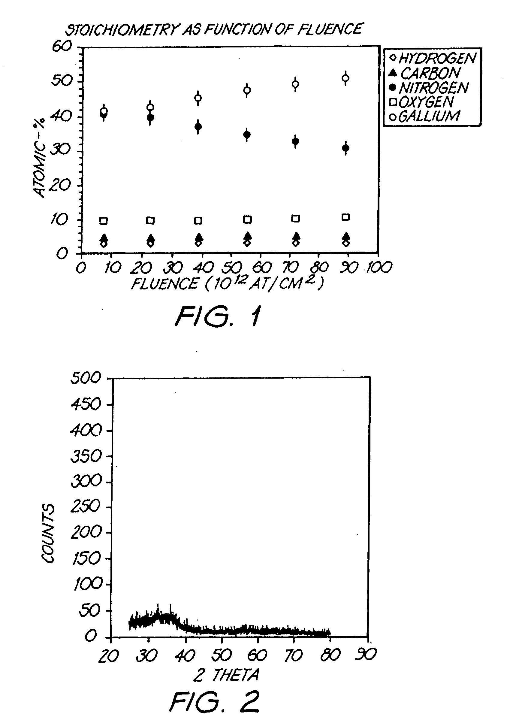
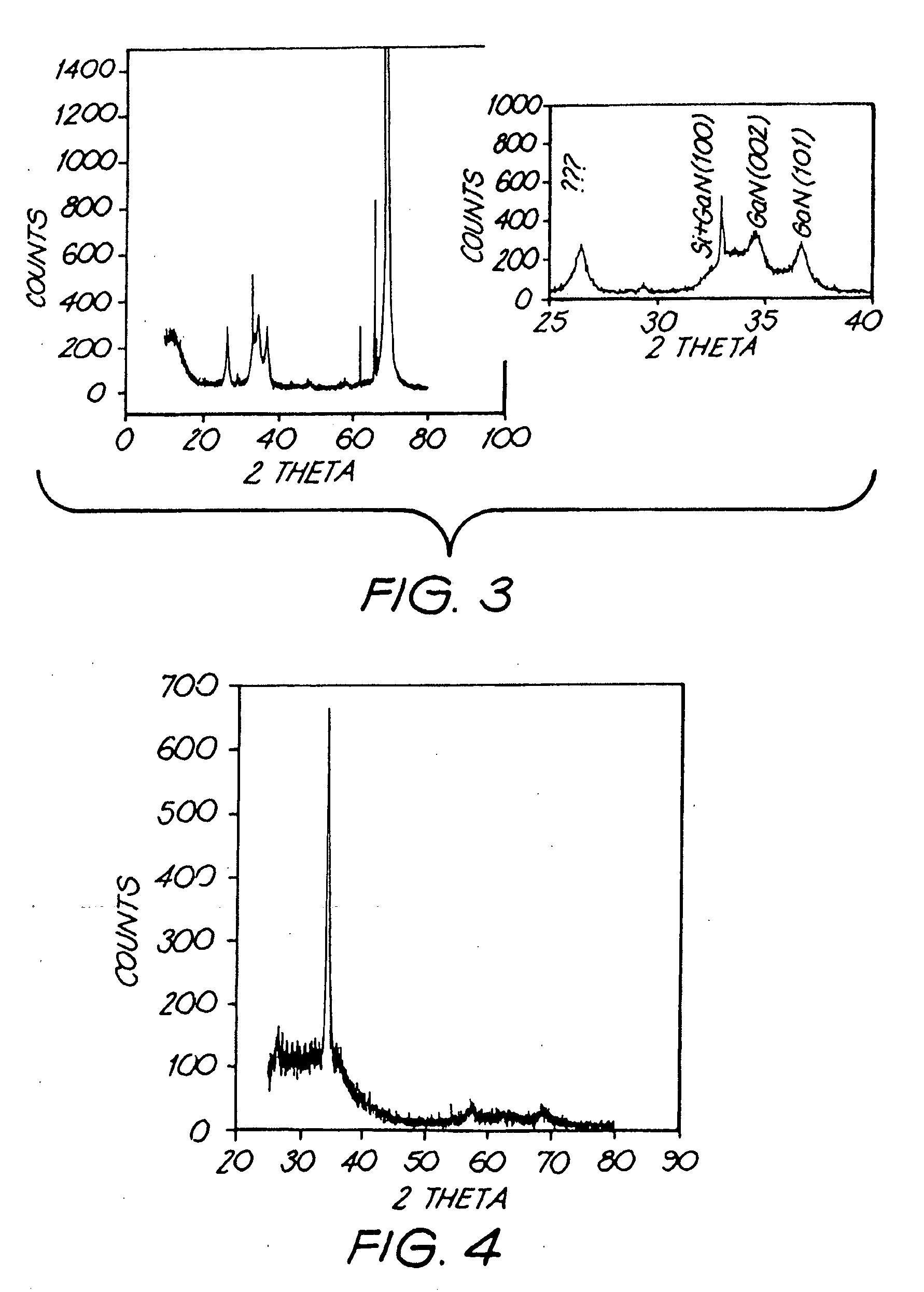
[0116]Of the fifteen films grown, three samples, which spanned the range of background vacuum levels used, were subjected to ERD analysis, as outlined below. These three samples were respectively ...

example 2

[0158]The attached pictures shows examples, by a number of different measurement techniques, of room temperature re-crystallization observed.

[0159]The pictures show a lot of small crystals, evidencing a polycrystalline nature shortly after growth, and a much less polycrystalline nature after two years.

example 3

Gallium Nitride Films Grown on Sapphire Substrates

[0160]Samples were grown on non-conducting sapphire substrates so that sample conductivity measurements could be made. The growth conductions used were the same as for the samples grown on silicon described in example 1 and 2 above.

[0161]Electrical measurements were made of the conductivity of samples of gallium nitride grown using the above technique. Some re-crystallization took place in a sample that was semi-insulating (resistivity more than 10,000 ohm-cm) shortly after growth and became much more conductive (86 ohm-cm) about two years later.

[0162]For the growth of this sample on sapphire, the above conditions produced gallium rich films under low oxygen conditions. A slightly yellow colouration was noted. This colouration was similar to that observed for gallium rich bulk grown gallium nitride [26].


PUM

PropertyMeasurementUnit
temperatureaaaaaaaaaa
resistivityaaaaaaaaaa

Abstract

A process for the manufacture of a gallium rich gallium nitride film is described. The process comprises (a) preparing a reaction mixture containing a gallium species and a nitrogen species, the gallium species and the nitrogen species being selected such that, when they react with each other, gallium nitride is formed; and (b) growing the gallium rich gallium nitride film from the reaction mixture, by allowing the gallium species to react with the nitrogen species and to deposit gallium nitride on a substrate selected from the group consisting of silicon, glass, sapphire, quartz and crystalline materials having a lattice constant closely matched to gallium nitride, including zinc oxide, optionally with a zinc oxide buffer layer, at a temperature of from about 480° C. to about 900° C. and in the presence of a gaseous environment in which the partial pressure of oxygen is less than 10−4 Torr, wherein the ratio of gallium atoms to nitrogen atoms in the gallium rich gallium nitride film is from 1.01 to 1.20. The invention also provides the option of annealing the gallium rich gallium nitride film at a temperature of from about 20° C. to about 650° C. and for a time sufficient to decrease the resistivity of the film so that it becomes electrically conductive, for instance to a resistivity below 100 ohm.cm.

Description

CROSS-REFERENCE TO RELATED APPLICATIONS[0001]This application is a divisional of U.S. application Ser. No. 10 / 514,772, filed on Jun. 20, 2005 which is the national stage entry of PCT / AU03 / 00598 filed on May 19, 2003 which claims priority to Australian Application No. PS 2404, filed on May 17, 2002. All of which are expressly incorporated herein by reference.TECHNICAL FIELD[0002]The present invention relates to the manufacture of materials suitable for use in lasers; ultraviolet light detectors and high power microwave transistor devices. More particularly, the invention relates to a process for the manufacture of a gallium nitride film and to a gallium nitride film manufactured by the process.BACKGROUND OF THE INVENTION[0003]Gallium nitride is a material widely used in the construction of blue, violet and white light emitting diodes, blue laser diodes, ultraviolet detectors and high power microwave transistor devices.[0004]Present gallium nitride device technology is based on what i...

Claims


Application Information

Patent Timeline
Patent Type & Authority Applications(United States)
IPC IPC(8): C23C16/00C01B21/06C01G15/00C23C16/02C23C16/30C23C16/34C30B25/02C30B25/10C30B29/40C30B33/02H01L21/205
CPCC01G15/00C01P2002/72C01P2004/03C23C16/0272C23C16/303C30B25/02C30B25/105C30B29/406C30B33/02Y10S148/004H01L33/00
Inventor BUTCHER, KENNETH SCOTT ALEXANDERTANSLEY, TREVOR LIONELAFIFUDDIN
Owner BUTCHER KENNETH SCOTT ALEXANDER
Why Eureka
Try Eureka