Nitride semiconductor laser chip and fabrication method thereof

a technology of semiconductor laser chips and semiconductors, applied in semiconductor lasers, lasers, active medium materials, etc., can solve the problems of nitride semiconductors, affecting the quality of individual chips, and a certain proportion of samples (individual chips actually fabricated) to break down, so as to improve crystal asymmetry, prevent damage to the facet, and improve the effect of reliability

Inactive Publication Date: 2008-12-04
SHARP KK
View PDF5 Cites 190 Cited by
  • Summary
  • Abstract
  • Description
  • Claims
  • Application Information

AI Technical Summary

Benefits of technology

[0027]According to the invention, the provision of an etched-in portion makes it possible to reset, with the etched-in portion, the step that develops on the resonator facet during cleaving. Thus, it is possible to reset the step at the etched-in portion, which is located close to the place where the step that develops at the resonance facet originates from, and it is thus possible to prevent development of a step at the stripe-shaped waveguide, where the emission of laser takes place. In this way, it is possible to prevent damage to the facet at the laser emission portion, and it is thus possible to fabricate a nitride semiconduct

Problems solved by technology

Disadvantageously, however, even a nitride semiconductor laser chip laminated on a nitride semiconductor substrate having the (1-100) plane as the principal plane as described above does not offer satisfactory characteristics: when such a chip is subjected to CW (continuous wave) lasing (continuous lasing) up to a high output, a certain proportion of its samples (individual chips actually fabricated) break down before reaching a satisfactory light output.
Moreover, with this conventional nitride semiconductor laser chip, the proportion of its samples that break down increases with the length of time for which they are driven.
Depending on the conditions under which they are driven, it may even occur that most samples of the nitride semiconductor laser chip fabricated offer unsatisfactory reliability.
This indicates that a nitride semiconductor laser chip laminated

Method used


Image

  • Nitride semiconductor laser chip and fabrication method thereof
  • Nitride semiconductor laser chip and fabrication method thereof
  • Nitride semiconductor laser chip and fabrication method thereof

Examples


Embodiment Construction

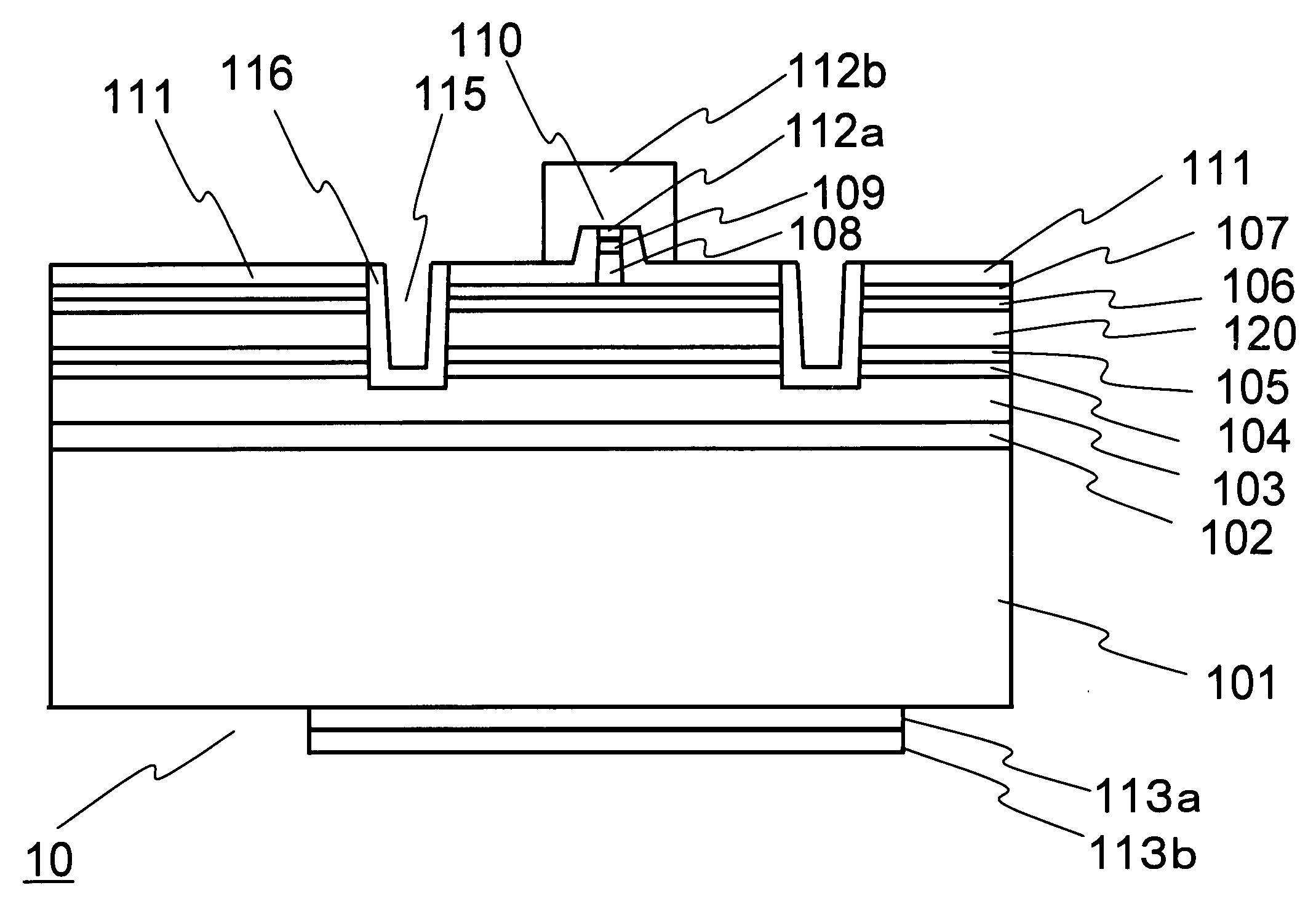
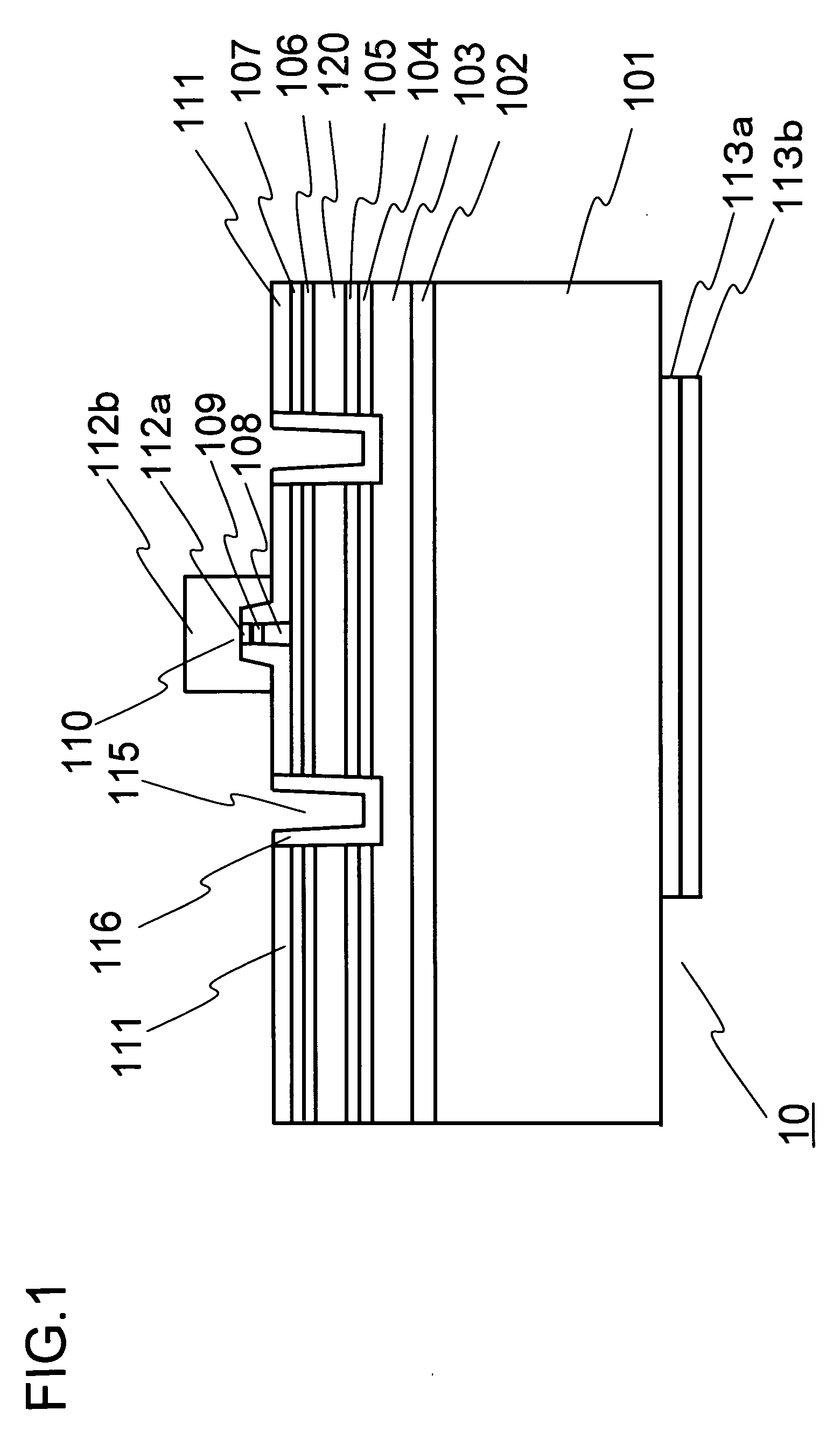
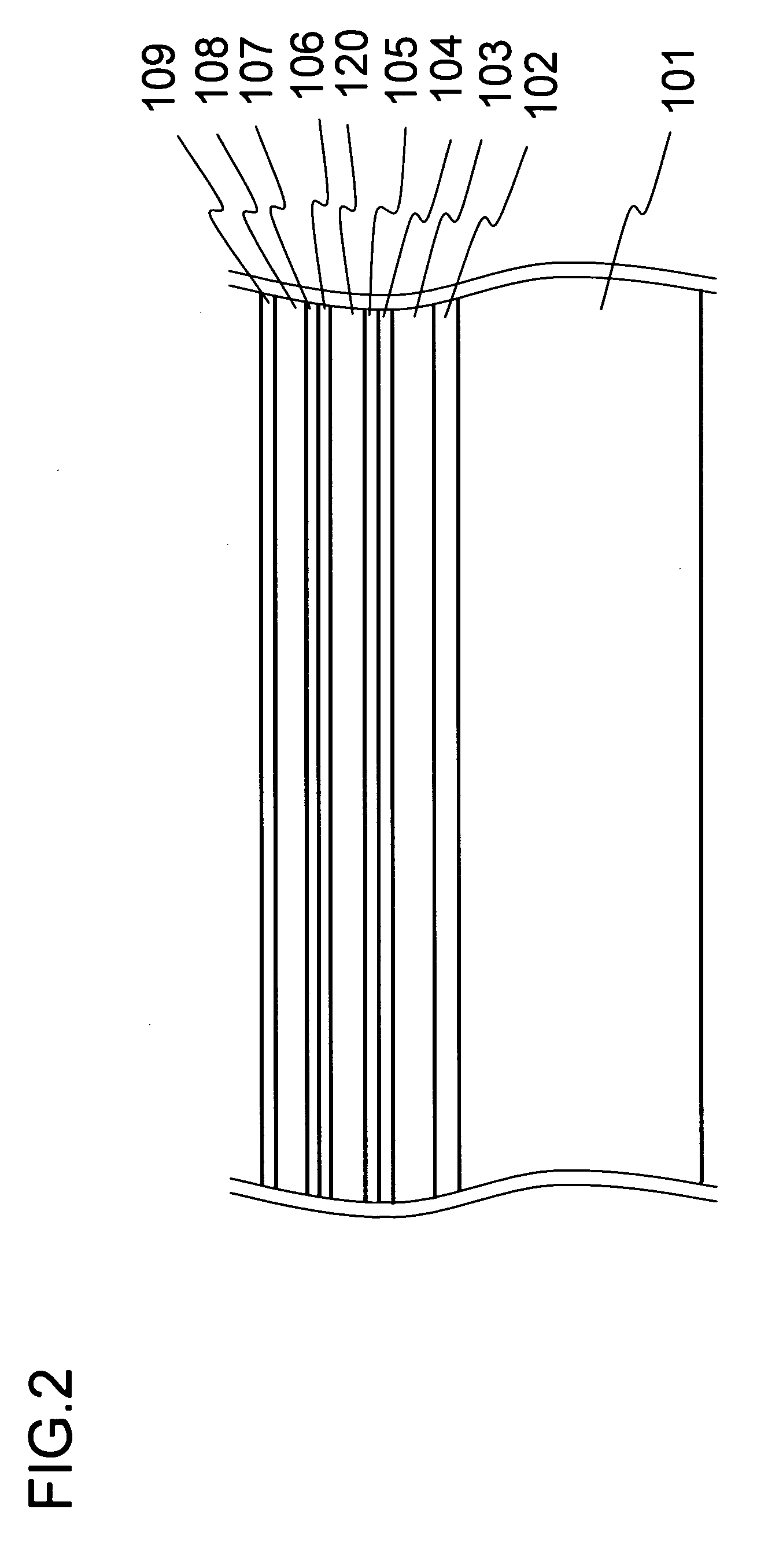
[0037]Hereinafter, an embodiment of the present invention will be described with reference to the accompanying drawings. FIG. 1 is a front view showing an outline of the structure of a nitride semiconductor laser chip. FIGS. 2, 3, and 5 are sectional views of a wafer illustrating the fabrication procedure of a nitride semiconductor laser chip. FIGS. 4 and 6 are top views of a wafer illustrating the fabrication procedure of a nitride semiconductor laser chip. FIG. 7 is a top view of a laser bar illustrating the fabrication procedure of a nitride semiconductor laser chip. FIG. 8 is an enlarged schematic view of a cleavage surface of a nitride semiconductor laser chip as a control example.

[0038]Formation of individual layers by epitaxial growth: On the surface of an n-type GaN substrate 101 having the (1-100) plane (also called the m-plane) as the principal plane for crystal growth, by a crystal growth technology such as MOCVD (metal-organic chemical vapor deposition), nitride semicond...


PUM


Abstract

In a nitride semiconductor laser chip so structured as to suppress development of a step on nitride semiconductor layers, the substrate has the (1-100) plane as the principal plane, the resonator facet is perpendicular to the principal plane, and, in the cleavage surface forming the resonator facet, at least by one side of a stripe-shaped waveguide, an etched-in portion is formed as an etched-in region open toward the surface of the nitride semiconductor layers.

Description

[0001]This nonprovisional application claims priority under 35 U.S.C. §119(a) on Patent Application No. 2007-144428 filed in Japan on May 31, 2007, the entire contents of which are hereby incorporated by reference.BACKGROUND OF THE INVENTION[0002]1. Field of the Invention[0003]The present invention relates to a nitride semiconductor laser chip and to a method for fabricating it. More specifically, the invention relates to a nitride semiconductor laser chip having nitride semiconductor layers laminated on a nitride semiconductor substrate having a particular planar orientation, and to a method for fabricating such a nitride semiconductor laser chip.[0004]2. Description of Related Art[0005]Nitride semiconductors are compounds of N (nitrogen), which is a group V element, with a group III element, such as Al (aluminum), Ga (gallium), and In (indium). For their band structures and chemical stability, nitride semiconductors have been receiving much attention as semiconductor materials for...

Claims


Application Information

Patent Timeline
IPC IPC(8): H01S5/22H01L33/00
CPCB82Y20/00H01S5/0201H01S5/0202H01S5/0425H01S5/22H01S5/3201H01S5/3202H01S5/34333H01S5/32025H01S5/04254
Inventor YAMASHITA, FUMIOITO, SHIGETOSHIYAMAMOTO, SHUICHIROKAWAKAMI, TOSHIYUKI
Owner SHARP KK
Why Eureka
Try Eureka