Printing of contact metal and interconnect metal via seed printing and plating

a technology of interconnecting metal and contact metal, which is applied in the direction of basic electric elements, semiconductor devices, electrical equipment, etc., can solve problems such as metal breakage or discontinuity, and achieve the effect of eliminating the need for etching, and reducing the number of processing steps

Active Publication Date: 2009-01-22
ENSURGE MICROPOWER ASA
View PDF8 Cites 32 Cited by
  • Summary
  • Abstract
  • Description
  • Claims
  • Application Information

AI Technical Summary

Benefits of technology

[0008]Optionally, different resistivities of the metal interconnect and the metal silicide contact can be achieved on a single substrate by altering the thickness of the printed metal. For example, thicker metal or more metal ink (achieved, for example, by increasing the number of drops, the drop volume or the ink volume, and / or decreasing the pitch between drops in a certain area) can be printed in areas where a lower resistance is desired. This technique has the marked advantage over conventional processing in that different thicknesses of material can be placed onto the substrate during the same processing step (e.g., printing). Optionally, the contact angle of the printed ink can be locally varied (for example, using a preprinting step, adapted to locally vary the surface energy of the substrate) so that different metal heights and line widths can be achieved with the same printing step.
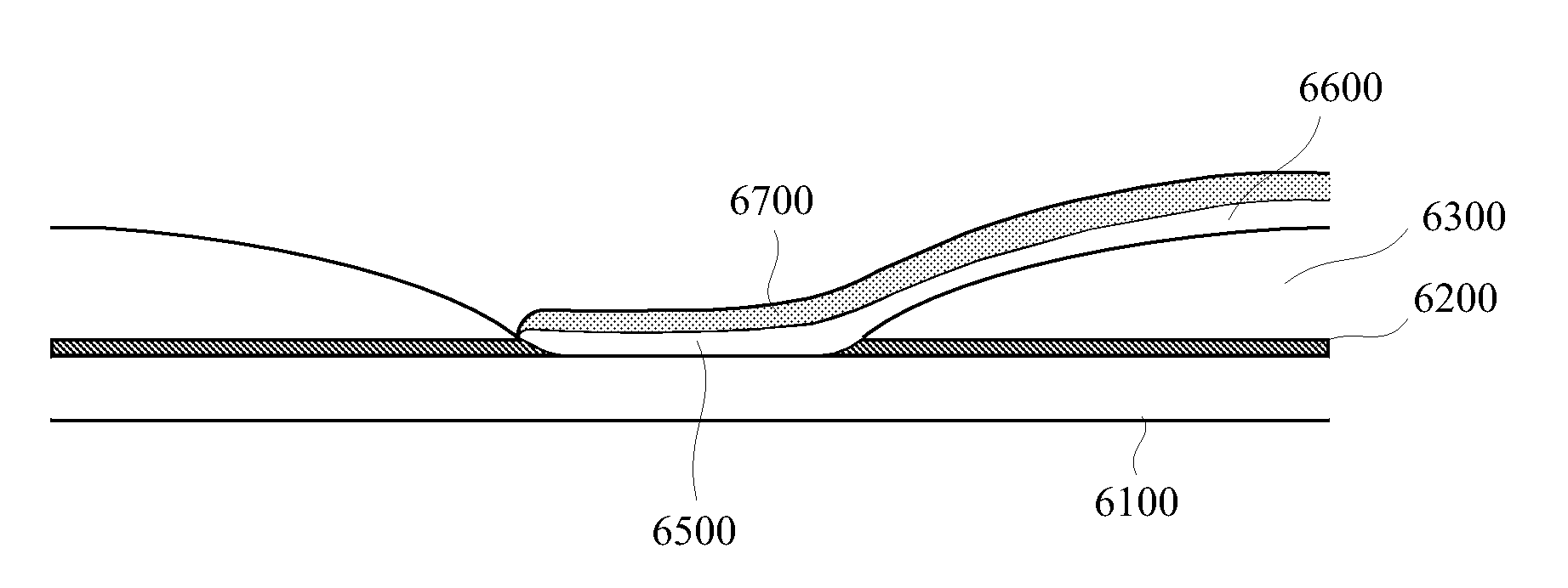
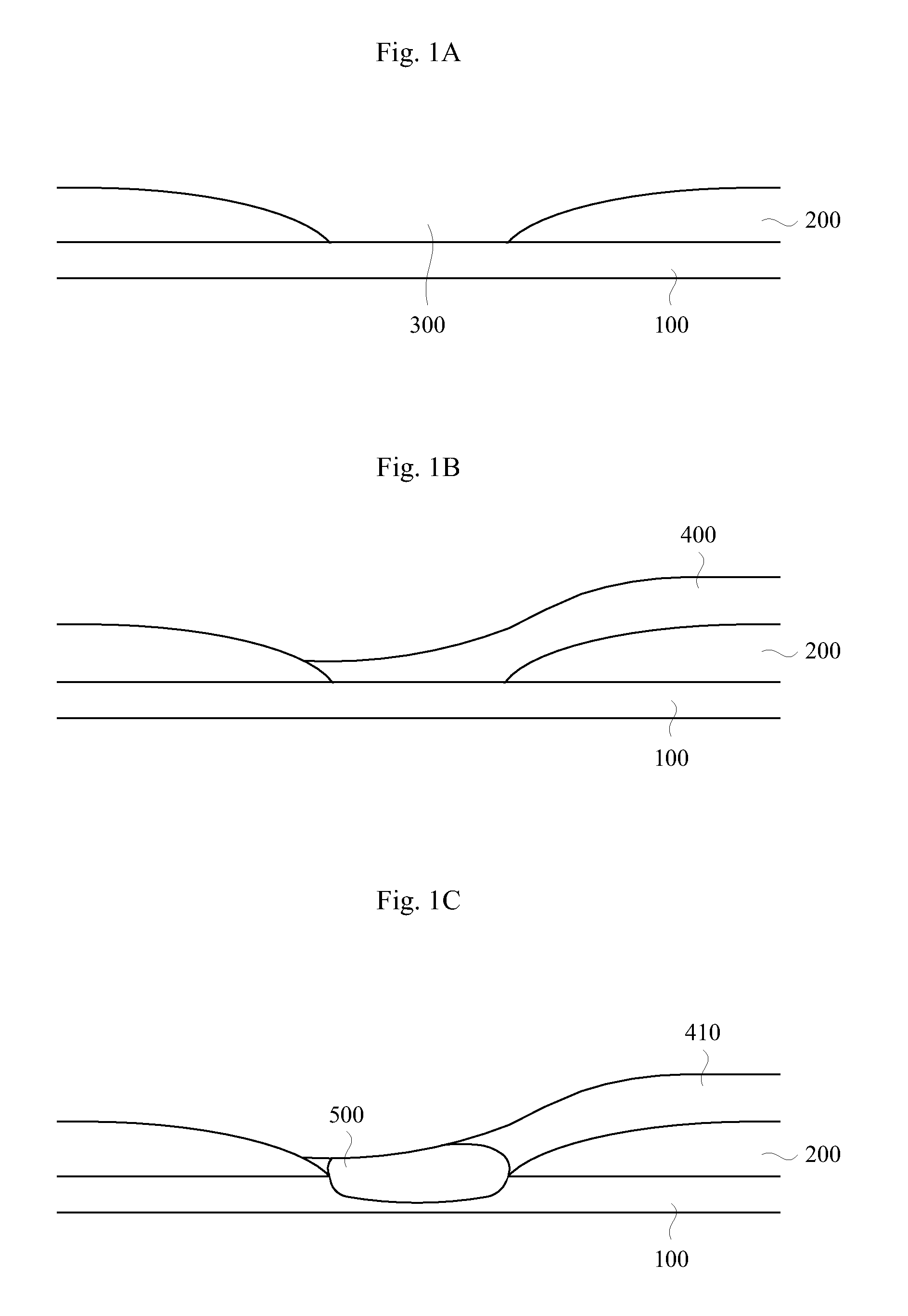
[0013]One important aspect of the present invention relates to the fabrication of a contact and a local interconnect in a single printing step using the metal precursor ink for both layers. This approach reduces the number of processing steps and does not require any etching steps. In the alternative, if different metals are desired for the contacts and the interconnect lines, a printed metal pattern (e.g., Pd) may be used as a seed layer for electroless deposition or electroplating of other metals (e.g., Ag, Cu, Ni, etc.), as well as for forming a metal silicide (e.g., Pd2Si) in the contact areas. The thickness of the metal and the curing process to form the silicide may be chosen or determined such that all of the metal in the contact area is not consumed, while good silicide contacts are still formed. Additional metal may be plated onto the metal seed layer and / or onto the metal silicide, in the interconnect areas and / or in the contact areas. An additional annealing step (e.g., post-plating) may further improve the electrical contact between the silicide and the plated metal. In this process, the printed and cured metal precursor film (e.g., to form the metal and metal silicide layers) does not have to be continuous. Additionally, a cleaning and / or roughening step, applied to the dielectric layer prior to printing the metal precursor ink, can improve the adhesion of the plated metal to the dielectric layer.
[0014]In various embodiments, a bulk conductive metal may be selectively deposited on any metal remaining after printing, drying and annealing the metal precursor ink. The bulk conductive metal may be deposited by plating the bulk conductive metal onto the remaining metal (i.e., from the ink). Plating the bulk conductive metal may comprise either electroless plating or electroplating, and the bulk conductive metal may be selected from the group consisting of Al, Ag, Au, Cu, Pd, Pt, Ni, Cr, Mo, W, Ru, Rh, and alloys and / or mixtures thereof. In some embodiments, the bulk conductive metal may be plated before or after silicide formation. In further embodiments, the bulk conductive metal may be further annealed (optionally, in the same step as silicide formation) to improve one or more physical and / or electrical characteristics of the bulk conductive metal.
[0022]The present invention provides a method of making contacts to silicon layers (and optionally, local interconnects) in electronic devices by the formation of a silicide from a metal precursor ink. The present invention also provides electronic devices such as diodes and transistors that include such contacts and / or local interconnects, and methods of forming such devices. By printing an ink containing a silicide-forming metal to form contacts and local interconnects at the same time, the number of processing steps may be reduced, and the need for etching may be reduced or eliminated. These and other advantages of the present invention will become readily apparent from the detailed description of preferred embodiments below.

Problems solved by technology

In conventional processing, depositing a metal by sputter deposition or electron beam evaporation over a sharp step can cause breaks or discontinuities in the metal.

Method used


Image

  • Printing of contact metal and interconnect metal via seed printing and plating
  • Printing of contact metal and interconnect metal via seed printing and plating
  • Printing of contact metal and interconnect metal via seed printing and plating

Examples


working examples

Formation of Contacts and Local Interconnects

[0085]The feasibility of metal silicide as a contact material was demonstrated with evaporated Pd. Palladium silicide (Pd2Si) formation overcame the presence of a surface oxide on the silicon and formed low resistance ohmic contacts to conventional and spincoated silicon films, thereby alleviating the need for special cleaning (e.g., a sputtering process) to clean contaminants from the silicon surface. The reaction between Pd and Si occurred at 300° C. in N2 or Ar / H2 as confirmed by x-ray diffraction, cross section SEM, and four point probe measurements. Functional via chains (contacts) using Pd2Si and Al interconnects were similarly demonstrated. Contact resistances in this case were about 10−6 ohm-cm2.


PUM

PropertyMeasurementUnit
temperatureaaaaaaaaaa

Abstract

Methods of forming contacts (and optionally, local interconnects) using an ink comprising a silicide-forming metal, electrical devices such as diodes and / or transistors including such contacts and (optional) local interconnects, and methods for forming such devices are disclosed. The method of forming contacts includes depositing an ink of a silicide-forming metal onto an exposed silicon surface, drying the ink to form a silicide-forming metal precursor, and heating the silicide-forming metal precursor and the silicon surface to form a metal silicide contact. Optionally, the metal precursor ink may be selectively deposited onto a dielectric layer adjacent to the exposed silicon surface to form a metal-containing interconnect. Furthermore, one or more bulk conductive metal(s) may be deposited on remaining metal precursor ink and / or the dielectric layer. Electrical devices, such as diodes and transistors may be made using such printed contact and / or local interconnects. A metal ink may be printed for contacts as well as for local interconnects at the same time, or in the alternative, the printed metal can act as a seed for electroless deposition of other metals if different metals are desired for the contact and the interconnect lines. This approach advantageously reduces the number of processing steps and does not necessarily require any etching.

Description

RELATED APPLICATIONS[0001]This application claims the benefit of U.S. Provisional Application No. 60 / 959,977, filed Jul. 17, 2007 (Attorney Docket No. IDR1051), which is incorporated herein by reference in its entirety.FIELD OF THE INVENTION[0002]The present invention generally relates to the field of semiconductor devices and methods of manufacturing the same. More specifically, embodiments of the present invention pertain to methods of forming electrical contacts (and optionally, local interconnects) using a metal ink, electrical devices such as diodes and / or transistors including such contacts and (optional) local interconnects, and methods for forming such devices.SUMMARY OF THE INVENTION[0003]Aspects of the present invention relate to methods of forming contacts to doped or undoped silicon layers, and optionally forming local interconnects, in electronic devices using a metal ink. Other aspects relate to electrical devices (e.g., diodes, transistors, etc.) including such contac...

Claims


Application Information

Patent Timeline
Patent Type & Authority Applications(United States)
IPC IPC(8): H01L21/768H01L21/28H01L29/78
CPCH01L21/28518H01L21/288H01L21/32051H01L21/32053H01L21/76838H01L21/76873H01L21/76895H01L2924/0002H01L29/458H01L29/78618H01L27/1285H01L27/1292H01L2924/00
Inventor CHANDRA, ADITIKAMATH, ARVINDCLEEVES, JAMES MONTAGUEROCKENBERGER, JOERGTAKASHIMA, MAOSCHER, ERIK
Owner ENSURGE MICROPOWER ASA
Why Eureka
Try Eureka