
Ultra high-resolution radiation detector (UHRD) and method for fabrication thereof

a radiation detector and ultra high-resolution technology, applied in the field of radiation detectors, can solve the problems of resolution, peak to background ratio, electrical drift field, and total depletion of semiconductor substrates, and achieve the effect of reducing the drift of pulse peak and low resolution

Inactive Publication Date: 2009-01-29
SHENZHEN SKYRAY INSTR
View PDF13 Cites 14 Cited by
  • Summary
  • Abstract
  • Description
  • Claims
  • Application Information

AI Technical Summary

Benefits of technology

[0019]An objective of the present invention is to provide an improved structure of the semiconductor electrodes for a semiconductor detector with better sensitivity, higher energy resolution and lower electronic noise that can operate at or near room temperature.
[0020]The objectives of the invention are achieved by designing a new shape of p-type drift electrode rings as a function of eliminating the damage in the depletion (effective) region of the semiconductor substrate.
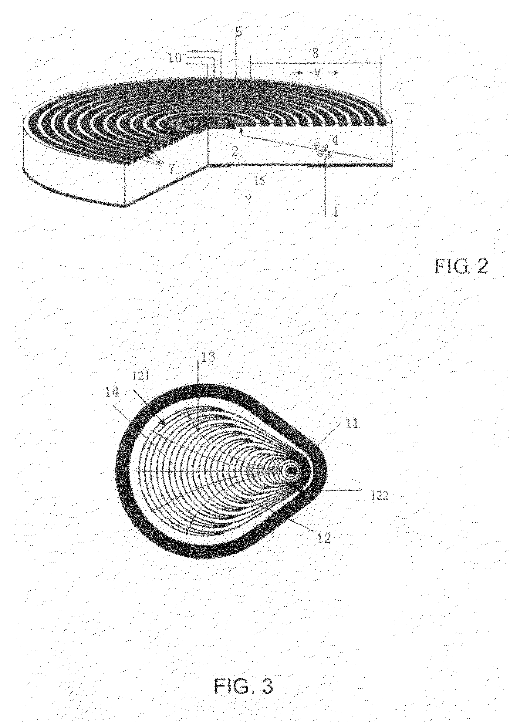
[0026]An advantage of the Semiconductor radiation detector according to The invention is the special p-type drift electrode rings which have a gibbous circularity topology. So the position of the FET and anode could be the region which outer of the depletion (effective) region, which could eliminate the erroneous figure of the X-ray spectrum by undesired signal charge damages.
[0029]Further advantageous refinements of the invention are characterized in the reset terminal, which could reduce the drift of the pulse peak and low resolution caused by the changeable large count rates radiation entrance. For example, when the count rates radiation entrance is 120 Kcps the drift of the pulse peak reduced to 0.24% comparing to the 0.92% of self-motion reset, while the energy resolution reduced to 3-4 ev comparing to the 40 ev of self-motion reset.

Problems solved by technology

Annular semiconductor electrodes (101) made of a strongly p-doped semiconductor material, in the effective region of the electrodes this results in total depletion of the semiconductor substrate, and also produces an electrical drift field in the semiconductor substrate.
However, the conventional SDD-based detector has several disadvantages.
First, a problem of appliances is the resolution and the peak to background ratio.
Since the field effect transistor is integrated onto the center of the semiconductor substrate, the electric field under the FET will twist, which would lead to erroneous figure of the X ray spectrum by undesired signal charge damages.
Though the FET occupied a small region of the detector's area, the damage in the sensitive region of the semiconductor substrate upon bonding may cause the detector to fail at high resolution and peak to background ratio.
As a result, the drift movement may reduce the input capacitance of the detector.
Third, since the resetting electrode is used to inject charges into the FET in order to reset it by release the leakage current of the FET.
When the rate at which X-ray photons hit the detector increases, also the leakage current increases, induces a drift of the X ray spectrum and results in low resolution which falsify the signals.

Method used


Image

  • Ultra high-resolution radiation detector (UHRD) and method for fabrication thereof
  • Ultra high-resolution radiation detector (UHRD) and method for fabrication thereof
  • Ultra high-resolution radiation detector (UHRD) and method for fabrication thereof

Examples


Embodiment Construction

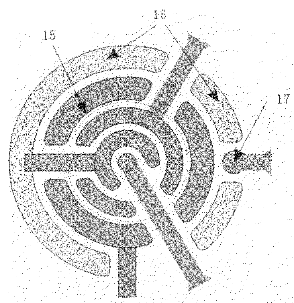
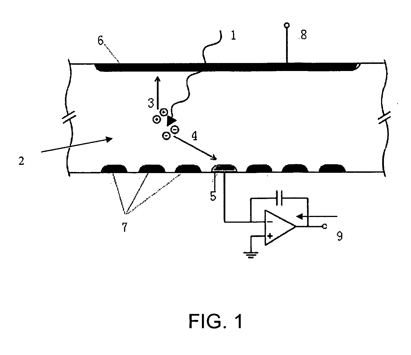
[0034]In the drawings: 1. entrance X-ray; 2. N-type Semiconductor chip and depletion (effective) region; 3. the holes produced by the entrance X-Ray radiation and its drift path; 4. the electrons produced by the entrance X-Ray radiation and its drift path; 105. anode; 102. source; 103. gate; 104. drain electrodes; 106. cathode; 6. the side of entrance X-Ray and P+ ion implanted layer; 101. the drift rings which formed by P+ ion implanted; 8. reverse bias voltage 9. amplifier; 10. Field Effect Transistor (FET); 11. the anode and the First Field effect transistor; 12. the p-type drift electrode rings which formed by P+ ion implanted; 13. the electrons produced by the entrance X-Ray radiation and its drift path; 14. the back side of the entrance X-Ray radiation; 15. the First Field effect transistor; 16. anode; 17. reset terminal; 121. the large circularity part of the p-type drift electrode rings which have gibbous circularity topology. 122. the small circularity part of the p-type dr...


PUM


Abstract

An ultra high-resolution radiation detector and method for fabrication thereof, has a detector chip, comprising the so-called drift rings and an amplifier integrated with the diode component, centrally located n-type anode on one surface, the depletion region. The detector chip has a circular field of view, the depletion region which also has a circular field of view by ion implanting symmetrical p-n junctions on the surface of the radiation entrance side of the detector chip, said centrally n-type anode located on the opposite surface of the depletion region, and its position is in the region which outer of the depletion region, said centrally n-type anode was surrounded by a plurality of p-type drift electrode rings, which have an gibbous circularity topology; wherein the focus of said p-type drift electrode rings is the position of the anode, said FET (Field-Effect Transistor) was integrated in the position of the detector's anode and directly coupled to the detector's anode. The p-type drift electrode rings is a plurality of drift rings which have gibbous circularity topology, wherein the gibbous circularity topology is encircled by a majority of a large circularity and a small circularity, wherein the maximum of the depletion region is the opposite surface of the region encircled by the outermost p-type drift electrode ring.

Description

TECHNICAL FIELD[0001]The invention concerns generally the technology of a radiation detector in the field of X-ray Fluorescence Spectrometer (XRF), more specifically the invention concerns an ultra high-resolution radiation detector (UHRD) and method for fabrication thereof.BACKGROUND OF THE INVENTION[0002]An energy dispersive X-ray fluorescence (EDXRF) spectrometer makes use of the fact that the pulse height of the detector signal is proportional to the X-ray photon energy, which is correlated with the wavelength. Therefore the optical path is simpler than for WDXRF spectrometers because no crystals or goniometry are needed and the fluorescence photons from the sample hit the detector directly. The samples are normally irradiated by X-rays from a tube with lower power than that used with the WDXRF spectrometers. The elements and their concentration are identified by counting the pulses at the different energy levels.[0003]The resolution of an EDXRF spectrometer depends strongly upo...

Claims


Application Information

Patent Timeline
IPC IPC(8): H01L31/0352H01L31/18
CPCH01L31/035281Y02E10/50H01L31/18H01L31/115
Inventor DONGLIANG, YAOSHENGHUI, LI
Owner SHENZHEN SKYRAY INSTR
Learn More