Method of depositing rare earth oxide thin films

a rare earth oxide and thin film technology, applied in the field of rare earth oxide thin film depositing, can solve the problems of low space densities on semiconductor-insulator interfaces, continuous decrease of electronic components, and lack of passivating and dielectric native oxide, and achieve the growth rate, morphology and crystallinity of films deposited according to the present invention. good, the effect of high growth rate of rare earth oxide thin film

Inactive Publication Date: 2009-02-05
ASM INTERNATIONAL
View PDF6 Cites 62 Cited by
  • Summary
  • Abstract
  • Description
  • Claims
  • Application Information

AI Technical Summary

Benefits of technology

[0026]It is an object of the present invention to eliminate the problems of the prior art and to provide a novel method of depositing rare earth oxide thin films by an ALD type process.
[0033]A number of considerable advantages are achieved with the aid of the present invention. Thus, considerably high growth rate of rare earth oxide thin films, for instance yttrium and lanthanum oxide thin films, are achieved at relatively low deposition temperature. Very cheap and safe source of oxygen, namely water, can be applied. The use of yttrium and lanthanum source chemicals of the present invention results in a growth rate of even five times faster compared to conventionally used thd compounds. Furthermore, the stoichiometry, morphology and crystallinity of the films deposited according to the present invention are better compared to films grown from the compounds. Generally it can be said, that smoothness of the Y2O3 thin films grown with new source materials is fully comparable with the smoothness of the films grown with Y(thd)3.

Problems solved by technology

One remarkable problem related to compound semiconductors is lack of passivating and dielectric native oxide (compare SiO2 on silicon).
So far, no other oxide has worked successfully in compound semiconductor MOSFETs (metal-oxide-semiconductor filed effect transistors) resulting in low space densities on semiconductor-insulator interface.
Continuous decrease of the size of the electronic components has set severe restrictions on the performance of the SiO2 gate oxide.
Reason to this is most commonly steric hindrances due to the size of the source material molecules.
However, the growth rate remained impractically low.
However, in the range of the self controlled growth the elemental contents correspond to those of La2O2CO3, indicating very poor quality of the resulted film because of the carbonate incorporation.

Method used


Image

  • Method of depositing rare earth oxide thin films
  • Method of depositing rare earth oxide thin films
  • Method of depositing rare earth oxide thin films

Examples


example 1

Deposition of Y2O3 Thin Films from (CpMe)3Y and Water

[0127]Deposition of the Y2O3 thin films were performed in a flow-type F-120 reactor manufactured by ASM Microchemistry Ltd. The schematic diagram of the reactor used is shown in FIG. 6. Reactor is provided with eight separate heating blocks. The source material was vaporized at the evaporation temperature in the first block and conveyed with the aid of pulsed carrier gas (N2) into the substrate space. Because of the increasing temperature gradient from the source to the substrate space the source material vapor did not condense on the conduit walls. The source material pulses were separated from each other by inert purging pulses (N2). Nitrogen gas was generated by a nitrogen gas generator (Nitrox UHPN 3000-1). Claimed purity of nitrogen was >99.999%. Deposition pressure was from 1 to 2 mbar. The deposition parameters, such as the number and length of pulses and temperatures of the heating blocks, were controlled by a computer.

[01...

example 2

Deposition of Y2O3 Thin Films from (CpMe)3Y and Ozone

[0141]Y2O3 films were grown according to Examples 1, except that ozone and a mixture of ozone and water were used instead of plain water as an oxygen source material.

[0142]Fischer Model 502 ozone generator (Fischer Labor-und Verfahrenstechnik GmbH, Meckenheim / Bonn, BRD) generated an ozone-oxygen mixture that had about 3.5% of ozone from pure oxygen (GA, 99.999%).

[0143]Si(100) and soda glass were used as substrates. Native oxide layer was not removed from the surface of the Si(100) substrate. The soda glass substrates were on the opposite side with respect to the Si(100) substrates.

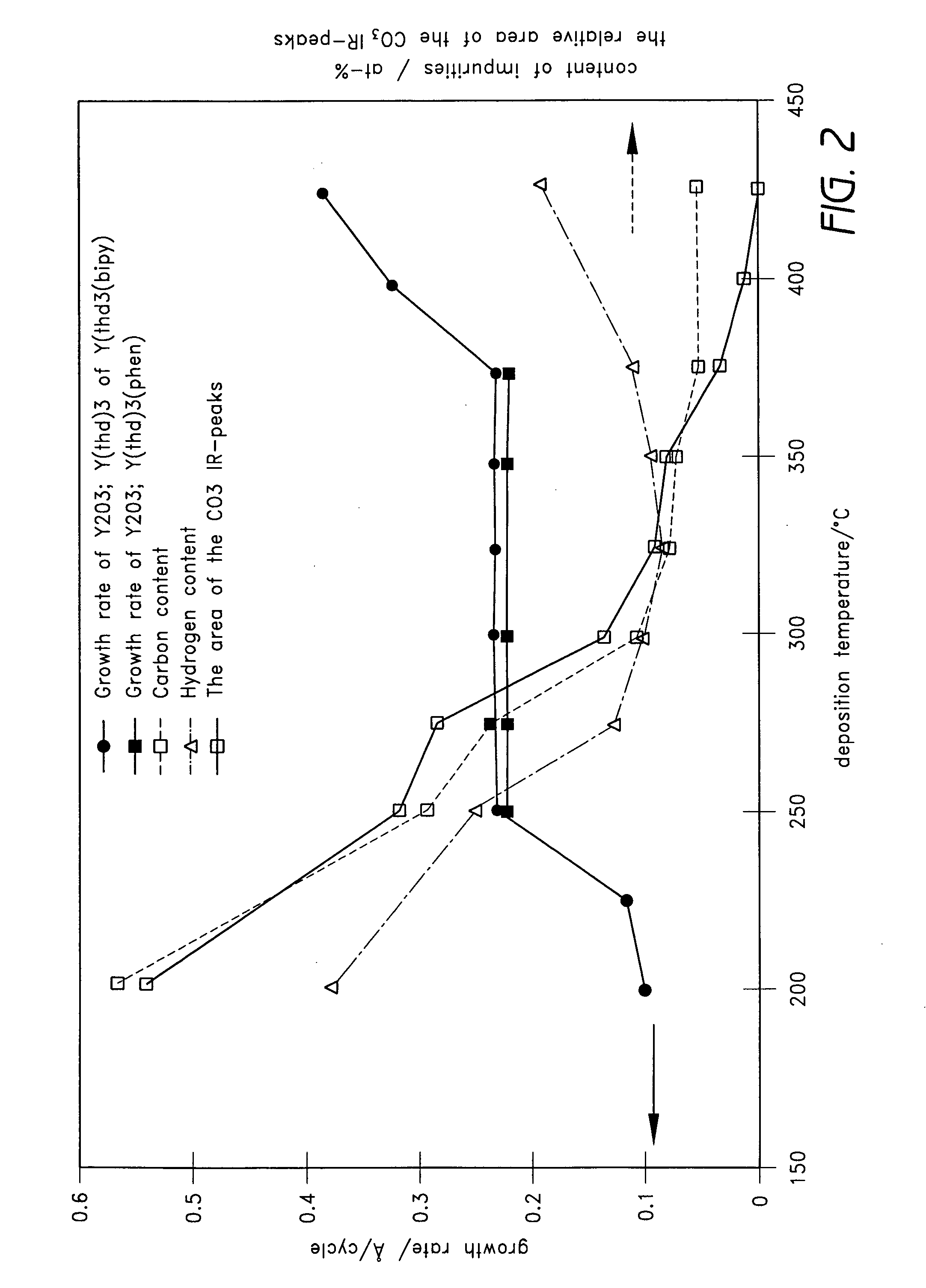
[0144]Changing the oxidant from water to a mixture of oxygen and ozone (pulsing time 2s) caused no change on the growth rate. However, when using a mixture of water and ozone, it was observed that a growth rate increased to 1.65 Å / cycle. That is about 30% higher than the value obtained at the same deposition temperature (300° C.) with plain water as the ...

example 3

Cp3Y as the Yttrium Source Material and Water as the Oxygen Source

[0148]The Cp3Y source material is sensitive to air like (CpMe)3Y. Thus, the handling of the source material, loading the source material boat, conveying to the reactor and determining an appropriate evaporation temperature was performed in the same ways as explained in experiment 1. Water was used as an oxidant for the deposition of the Y2O3 thin films.

[0149]In order to define an ALD window, depositions of the Y2O3 thin films were performed at temperature range from 200 to 400° C. In order to evaluate the linearity of the growth rate the number of the deposition cycles was varied from 300 to 4000 at a deposition temperature of 300° C. The effect of the length of the source material pulses was studied in the deposition temperature range from 200 to 300° C.

[0150]Cp3Y was evaporated at 150-155° C. The length of the pulses of Cp3Y and water was 0.7 s and the purging pulses between the source material pulses were 1.0 and 1...


PUM

PropertyMeasurementUnit
pressureaaaaaaaaaa
pressureaaaaaaaaaa
temperatureaaaaaaaaaa

Abstract

The present invention concerns a process for depositing rare earth oxide thin films, especially yttrium, lanthanum and gadolinium oxide thin films by an ALD process, according to which invention the source chemicals are cyclopentadienyl compounds or rare earth metals, especially those of yttrium, lanthanum and gadolinium. Suitable deposition temperatures for yttrium oxide are between 200 and 400° C. when the deposition pressure is between 1 and 50 mbar. Most suitable deposition temperatures for lanthanum oxide are between 160 and 165° C. when the deposition pressure is between 1 and 50 mbar.

Description

REFERENCE TO RELATED APPLICATIONS[0001]The present application is a continuation of U.S. patent application Ser. No. 10 / 067,634, filed Feb. 4, 2002 and claims priority to Japanese Patent Application Number 2001-236874, filed Aug. 3, 2001.BACKGROUND OF THE INVENTION[0002]1. Field of the Invention[0003]The present invention relates to a method of depositing rare earth oxide thin films. In particular, the invention concerns a method of growing yttrium, gadolinium and lanthanum oxide thin films by Atomic Layer Deposition (referred to as ALD hereinafter).[0004]ALD has previously been known as Atomic Layer Epitaxy (ALE) and later more specifically as Atomic Layer Chemical Vapor Deposition (Atomic Layer CVD™ and ALCVD™) process which are trademarks of ASMI®. ALD has been adopted as a general name of the method to avoid possible confusion when discussing about polycrystalline and amorphous thin films. Other names used in the literature for ALD are digital epitaxy, digital layer epitaxy (DLE...

Claims


Application Information

Patent Timeline
Patent Type & Authority Applications(United States)
IPC IPC(8): H01L21/44C01F17/00C23C16/40C23C16/44C23C16/455C30B29/16H01L21/316
CPCC23C16/40C23C16/45553C23C16/405
Inventor NIINISTO, JAAKKOPUTKONEN, MATTIRITALA, MIKKORAISANEN, PETRINISKANEN, ANTTILESKELA, MARKKU
Owner ASM INTERNATIONAL
Why Eureka
Try Eureka