

Semiconductor Device and Manufacturing Method Thereof
- Summary
- Abstract
- Description
- Claims
- Application Information
AI Technical Summary
Benefits of technology
Problems solved by technology
Method used
Image

Examples
exemplary embodiment 1
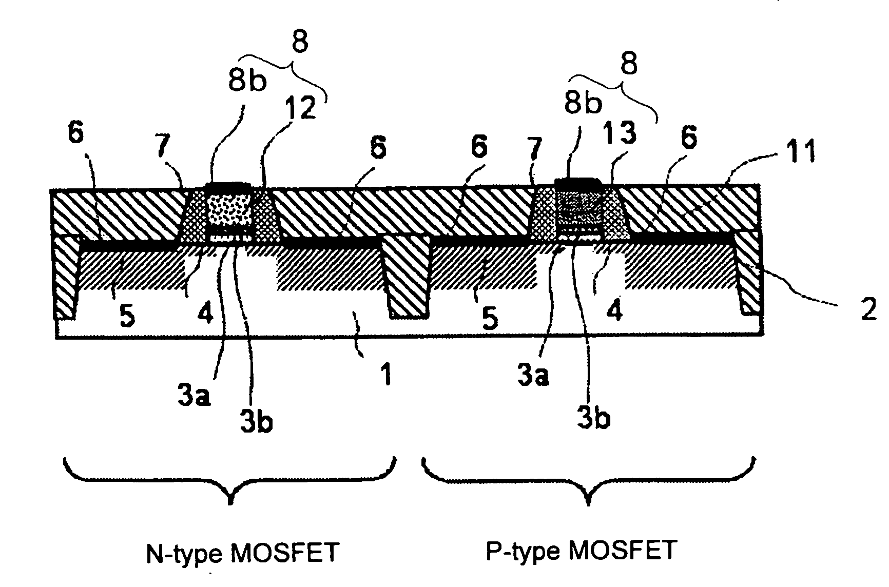
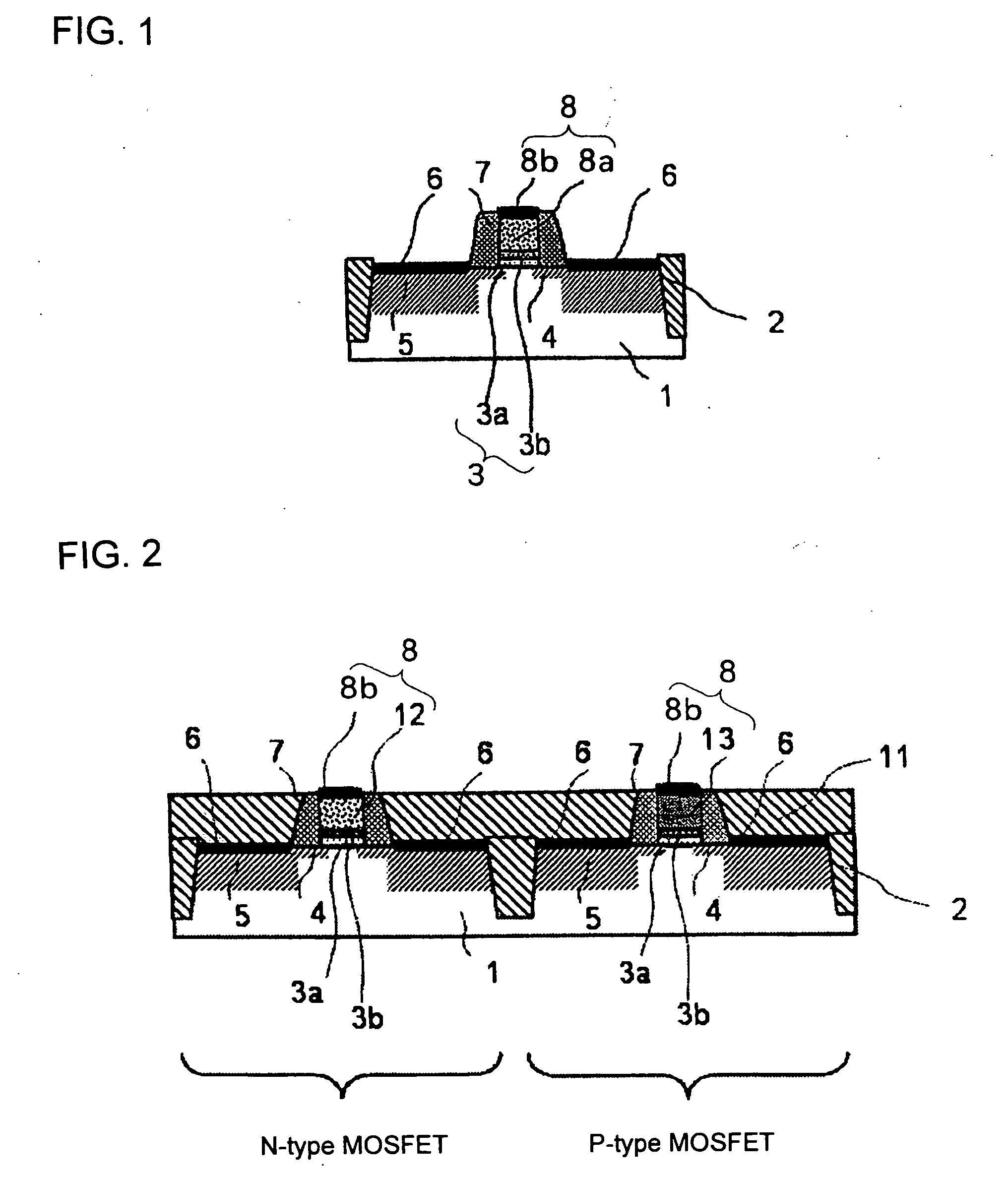
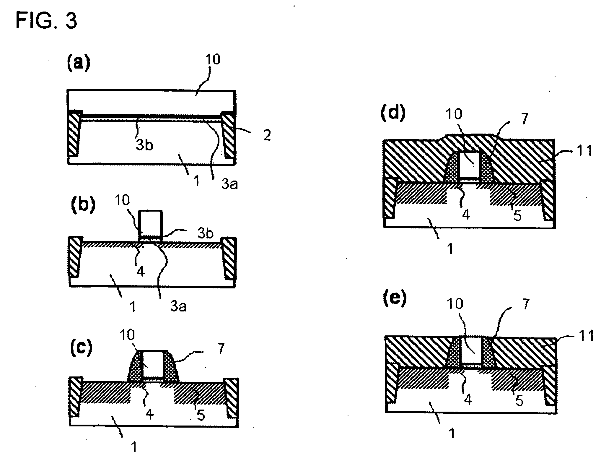
[0147]This exemplary embodiment is an example in which an NiSi2 phase is formed in the gate electrode lower part, and an NiSi phase, in the upper part. FIGS. 3 (a) through (e) and FIGS. 4 (f) through (l) show sectional views of a MOSFET manufacturing process pertaining to this exemplary embodiment.
[0148]First, as shown FIG. 3(a), an element isolating region 2 was formed in the surface region of the silicon substrate 1 by using an STI (Shallow Trench Isolation) technique. Then, the gate insulating film 3 (3a and 3b) was formed over the surface of the element-isolated silicon substrate. This gate insulating film had a structure comprising a silicon oxide film 3a and a high dielectric constant insulating film 3b. This exemplary embodiment used a gate insulating film having an HfSiON and SiO2 composition in which the Hf concentration in the gate insulating film varied in the depthwise direction, the Hf concentration was the highest in the vicinities of the interface between the gate ele...
exemplary embodiment 2
[0163]This is an example in which an Ni3Si phase is formed in the gate electrode lower part, and an NiSi phase, in the upper part. FIGS. 5 (a) through (f) and FIGS. 6 (g) through (l) show sectional views of a MOSFET manufacturing process pertaining to this exemplary embodiment.
[0164]First, the upper part surface of the polycrystalline silicon film 10 for gate use is exposed as shown in FIG. 5(a) by executing a similar process to that for Exemplary Embodiment 1 described with reference to FIGS. 3(a) through (e) above.
[0165]Then, the height of the polycrystalline silicon film 10 is reduced to half or less of that of the interlayer insulating film 11 by dry etching (FIG. 5(b)). This is done because formation of the Ni3Si layer by full silicidation technique lets the volume expansion due to silicidation make the height of the Ni3Si layer double that of the polycrystalline silicon film 10 before the silicidation or even higher. If the height of the polycrystalline silicon film 10 is set ...
exemplary embodiment 3
[0179]This is an example of fabricating a CMOS device in which an NiSi2 phase is used in the gate electrode of the N-type MOSFET, and an Ni3Si phase, in the gate electrode of the P-type MOSFET. FIG. 7 through FIG. 11 show sectional views of a MOSFET manufacturing process pertaining to this exemplary embodiment.
[0180]First, the upper part surface of the polycrystalline silicon film 10 for gate use is exposed as shown in FIG. 7(a) by executing a similar process to that for Exemplary Embodiment 1 described with reference to FIGS. 3(a) through (e) above.
[0181]Next, a diffusion preventive layer 20 was deposited all over the wafer where the upper part surface of the polycrystalline silicon film 10 was exposed. This diffusion preventive layer 20 is intended to prevent metal from a first metal film 19 for forming the silicide electrode of the N-type MOSFET from being diffused into the polycrystalline silicon film in the P-type MOSFET region. It is required for this diffusion preventive laye...
PUM
 Abstract
Description
Claims
Application Information