Semiconductor-on-insulator substrate with a diffusion barrier

a technology of diffusion barrier and semiconductor, applied in the direction of semiconductor devices, semiconductor/solid-state device details, electrical apparatus, etc., can solve the problems of high interface trap density and charge in the buried oxide layer

Inactive Publication Date: 2009-04-23
TAIWAN SEMICON MFG CO LTD
View PDF20 Cites 17 Cited by
  • Summary
  • Abstract
  • Description
  • Claims
  • Application Information

AI Technical Summary

Benefits of technology

[0010]The present invention addresses the needs described above by providing a semiconductor-on-insulator substrate containing a diffusion barrier layer for preventing diffusion of dopants into a buried insulator layer, and methods of manufacturing the same.

Problems solved by technology

Such materials provide less charge trapping than a silicon nitride layer, which causes a high level of interface trap density and charge in the buried oxide layer.

Method used


Image

  • Semiconductor-on-insulator substrate with a diffusion barrier
  • Semiconductor-on-insulator substrate with a diffusion barrier
  • Semiconductor-on-insulator substrate with a diffusion barrier

Examples


first embodiment

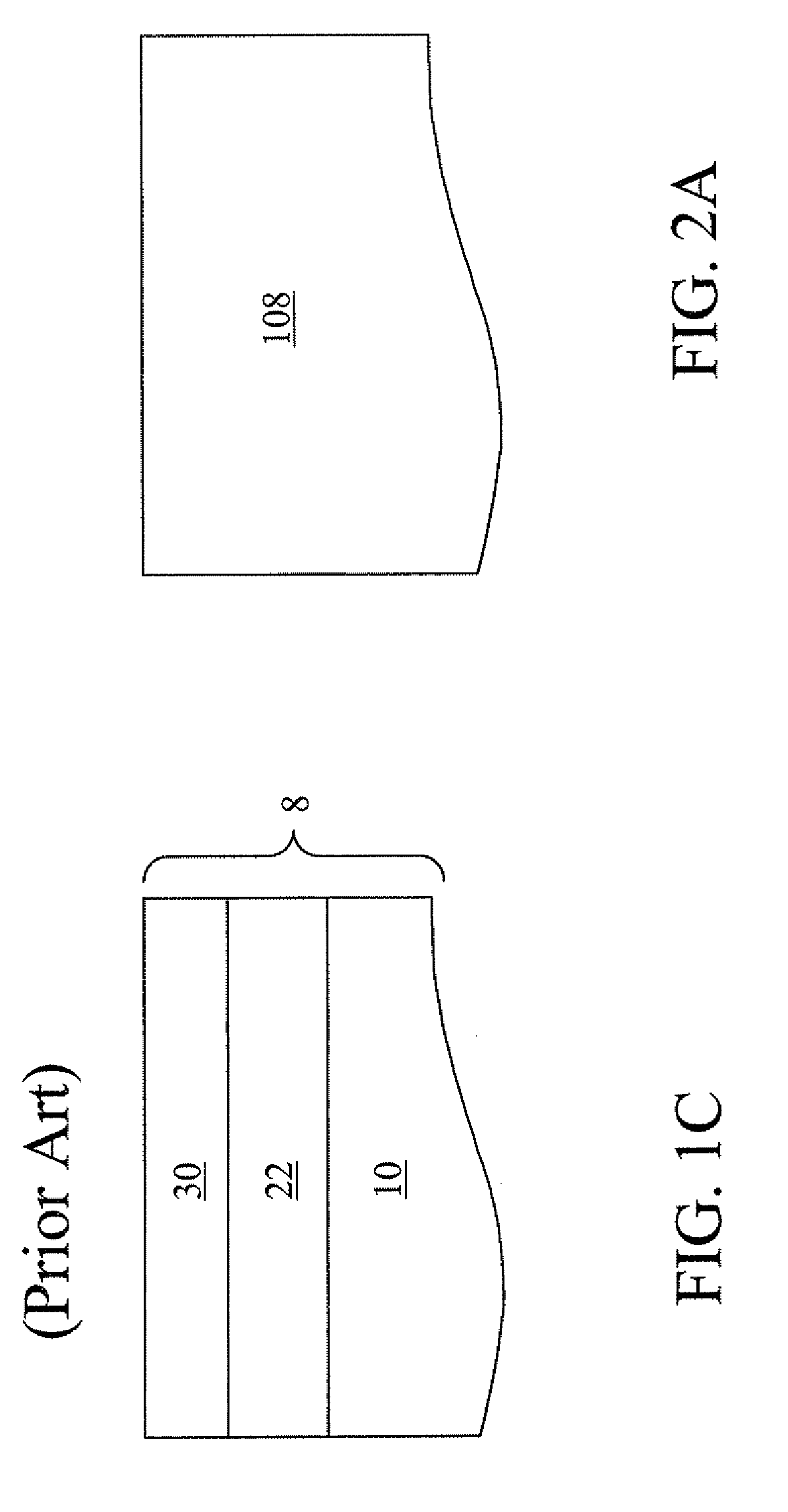
[0048]Referring to FIG. 2A, a first exemplary semiconductor structure according to the present invention comprises a semiconductor substrate 108. The semiconductor substrate 108 may be a bulk substrate at this point. The semiconductor substrate 108 comprises a semiconductor material such as silicon, a silicon germanium alloy, a silicon carbon alloy, a silicon germanium carbon alloy, a III-V compound semiconductor material, or a II-VI compound semiconductor material. The semiconductor material forms an insulating oxide when reacted with oxygen.

[0049]Referring to FIG. 2B, molecular oxygen ions (O2+) or atomic oxygen ions (O+) are implanted into the semiconductor substrate 108 in a high dose. Methods of forming a buried oxide layer by implanting oxygen ions followed by an anneal to form a buried oxide layer are known in the art as separation by ion implantation of oxygen (SIMOX). The molecular oxygen ions (O2+) or atomic oxygen ions (O−) are implanted into the semiconductor substrate e...

second embodiment

[0060]Referring to FIG. 3A, a second exemplary semiconductor structure according to the present invention comprises a first semiconductor substrate 208 which contains a first semiconductor layer 210. An oxide layer 222 and an oxynitride layer 224 are formed in the first semiconductor substrate 208. The oxide layer 222 may be formed by thermal oxidation of the semiconductor material in a top portion of the first semiconductor layer 210, and the oxynitride layer 224 may be formed by diffusing a nitridating gas through the oxide layer 222 and causing reaction of the nitridating gas with the semiconductor material in the first semiconductor layer 210 at an interface with the first semiconductor layer.

[0061]The thermal oxidation of the top portion of the first semiconductor layer 210 to form the oxide layer 222 and formation of the oxynitride layer 124 may be concurrent or sequential. In case the oxide layer 222 and the oxynitride layer 224 are formed concurrently, the first semiconducto...

third embodiment

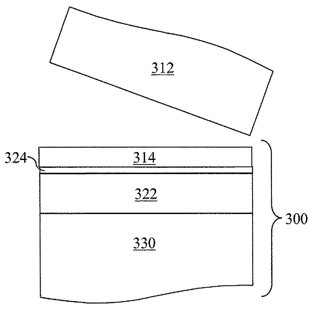
[0071]Referring to FIG. 4A, a third exemplary semiconductor structure according to the present invention comprises a first semiconductor substrate 308 that contains a first semiconductor layer 310 and a diffusion barrier layer 324. The diffusion barrier layer 324 may comprise a high-k dielectric material having a dielectric constant greater than 3.9 or silicon carbide. A high-k dielectric material may be a metal oxide, a metal oxynitride, a metal silicate, and alloys, mixtures, or multilayers of the same. The high-k dielectric materials are typically referred to as high-k gate dielectric materials, which are employed in advanced semiconductor devices to enable scaling of state-of-the-art field effect transistors. Non-limiting examples of the high-k dielectric materials include hafnium oxide, hafnium silicon oxide, lanthanum oxide, lanthanum aluminum oxide, zirconium oxide, zirconium silicon oxide, tantalum oxide, titanium oxide, barium strontium titanium oxide, barium titanium oxide...


PUM

PropertyMeasurementUnit
dielectric constantaaaaaaaaaa
thicknessaaaaaaaaaa
dielectric constantaaaaaaaaaa

Abstract

A diffusion barrier layer is incorporated between a top semiconductor layer and buried oxide layer. The diffusion barrier layer blocks diffusion of dopants into or out of buried oxide layer. The diffusion barrier layer may comprise a dielectric material such as silicon oxynitride or a high-k gate dielectric material. Alternately, the diffusion barrier layer may comprise a semiconductor material such as SiC. Such materials provide less charge trapping than a silicon nitride layer, which causes a high level of interface trap density and charge in the buried oxide layer. Thus, diffusion of dopants from and into semiconductor devices through the buried oxide layer is suppressed by the diffusion barrier layer without inducing a high interface trap density or charge in the buried oxide layer.

Description

FIELD OF THE INVENTION[0001]The present invention generally relates to semiconductor structures, and particularly to a semiconductor-on-insulator (SOI) substrate having a diffusion barrier layer between a top semiconductor layer and a buried insulator layer and methods of manufacturing the same.BACKGROUND OF THE INVENTION[0002]Semiconductor-on-insulator (SOI) devices are increasingly employed in high performance semiconductor chips for superior performance to bulk semiconductor devices. The SOI devices require a semiconductor-on-insulator (SOI) substrate including a buried insulator layer that provides electrical isolation to a top semiconductor layer from an underlying handle substrate.[0003]Relative to a bulk substrate, the SOI substrate provides benefits such as lower parasitic capacitance and resistance to latch up. As for reduction of parasitic capacitance, a handle substrate is separated from a top semiconductor layer by the buried insulator layer so that the distance of capac...

Claims


Application Information

Patent Timeline
Patent Type & Authority Applications(United States)
IPC IPC(8): H01L21/84H01L23/58H01L21/425
CPCH01L21/76254H01L21/76243
Inventor LEE, JUNEDONGSCHEPIS, DOMINIC J.SLEIGHT, JEFFREY W.REN, ZHIBIN
Owner TAIWAN SEMICON MFG CO LTD
Why Eureka
Try Eureka