Semiconductor-Nanoparticle-Dispersed Small Glass Particles and Process for Preparing the same

a technology of semiconductor nanoparticles and glass particles, which is applied in the field of small glass particles with dispersed semiconductor nanoparticles and process for preparing the same, can solve the problems of attracting attention, semiconductor nanoparticles whose fluorescence intensity reduction with time is small, and not always satisfactory in terms of brightness and color rendering properties, etc., to achieve excellent mechanical strength, increase fluorescence intensity, and excellent chemical stability against the external atmosphere

Inactive Publication Date: 2009-04-30
NAT INST OF ADVANCED IND SCI & TECH
View PDF8 Cites 31 Cited by
  • Summary
  • Abstract
  • Description
  • Claims
  • Application Information

AI Technical Summary

Benefits of technology

[0115]The semiconductor nanoparticle-dispersed small glass particles of the invention can emit various colors in the visible to near-infrared regions, particularly in the visible region, under UV radiation of the same wavelength according to the composition and particle size of the dispersed nanoparticles, when the particles are dispersed in a solution or formed into a powder by distilling off the solvent. The semiconductor-nanoparticle-dispersed small glass particles emit light with a fluorescence quantum yield of at least 25%, more preferably 60% or more, which is remarkably high, compared to known particles, and contain plural nanoparticles per glass particle, i.e., contains nanoparticles in a high concentration, thus providing increased fluorescence intensity. Furthermore, the semiconductor-nanoparticle-dispersed small glass particles as a whole basically have glass characteristics, and thus have excellent chemical stability against the external atmosphere, excellent mechanical strength, excellent heat resistance, etc., thus having excellent long-term stability of fluorescence characteristics.
[0116]The present invention further provides a process for producing fluorescent small glass particles that emit fluorescent light with high fluorescence quantum yield and has excellent long-term stability of fluorescence characteristics, which are due to the presence of plural semiconductor nanoparticles dispersed and fixed inside a small glass particle, as described above.

Problems solved by technology

However, such fluorescent materials are not always satisfactory in terms of brightness and color-rendering properties.
Even in such an application field, semiconductor nanoparticles whose fluorescence intensity reduction with time is small, compared to that of the organic dyes used so far, are attracting attention.
However, the semiconductor nanoparticles produced in a solution gradually aggregate, which starts immediately after the production, thus resulting in the deterioration of light emission characteristics.
The nanoparticles produced in a non-aqueous solution have particularly poor resistance to water, and the fluorescence is rapidly reduced in the presence of even a trace amount of water.
Another problem is that nanoparticle solutions, as is, are not suitable for technological applications.
In any case, the fluorescence quantum yield is as low as 20% or less, and unsatisfactory for practical use.
When semiconductor nanoparticles are fixed near the outer surfaces of the glass particles, shielding of the semiconductor nanoparticle from the external atmosphere is insufficient, compared to semiconductor nanoparticles fixed inside the glass.
Therefore, long-term stability of fluorescence characteristics tends to be insufficient.
However, because the nanoparticles are present only near the surface layer of the glass particle and the core of the glass particle does not contain nanoparticles, it is impossible to increase the concentration of nanoparticles dispersed in the glass particle, and it is thus difficult to obtain strong luminescence and high fluorescence quantum yield.
However, this method has the following disadvantage for practical use.
Because only one semiconductor nanoparticle can be contained in one small glass particle, the concentration of nanoparticles in the glass particles is very low, and it is difficult to obtain bright fluorescence.

Method used


Image

  • Semiconductor-Nanoparticle-Dispersed Small Glass Particles and Process for Preparing  the same
  • Semiconductor-Nanoparticle-Dispersed Small Glass Particles and Process for Preparing  the same
  • Semiconductor-Nanoparticle-Dispersed Small Glass Particles and Process for Preparing  the same

Examples


example 1

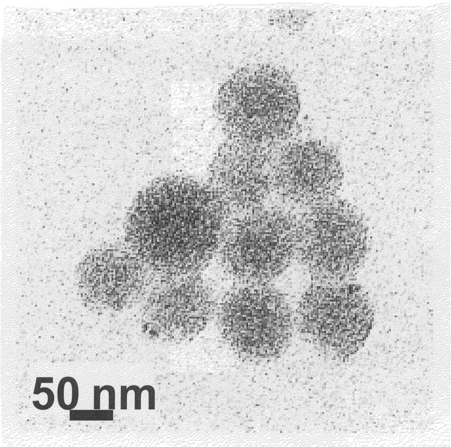
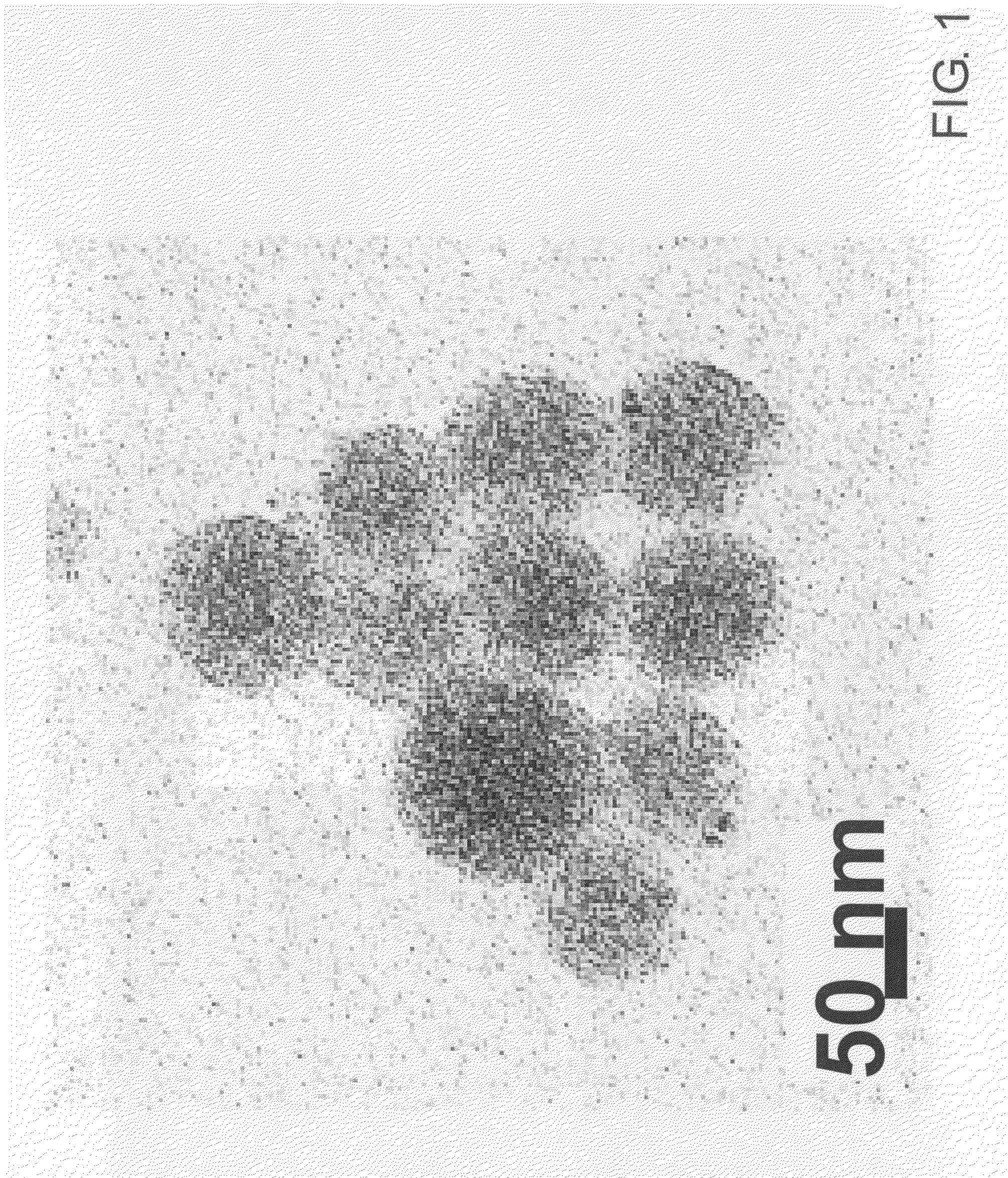
[0118]II-VI semiconductor cadmium telluride nanoparticles were prepared according to the method described in Li, Murase, Chemistry Letters, vol. 34, page 92 (2005). More specifically, while vigorously stirring an aqueous solution of cadmium perchlorate adjusted to pH 11.4, hydrogen telluride gas was allowed to react in the presence of thioglycolic acid (HOOCCH2SH) as a surfactant under an argon gas atmosphere. Clusters of cadmium telluride were thereby produced in the aqueous solution, and this aqueous solution was refluxed under atmospheric pressure for 6 days, thus providing cadmium telluride nanoparticles having a mean particle size of 4 nm and emitting red light with an emission peak wavelength of 646 nm under UV excitation and with a fluorescence quantum yield of 81%.

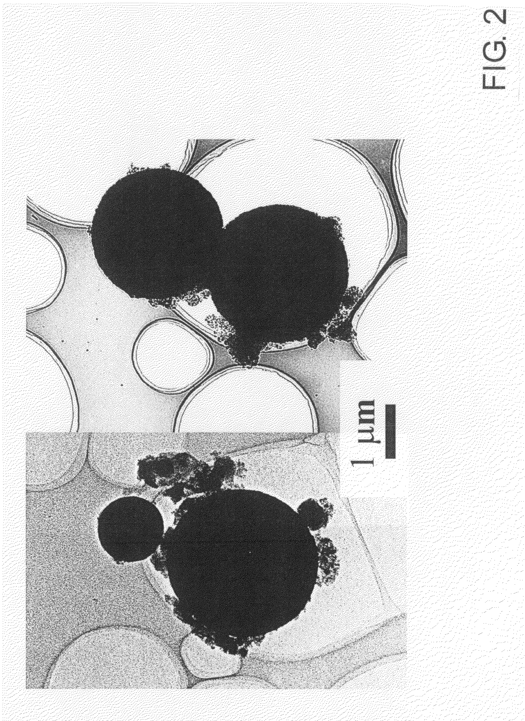
[0119]The semiconductor nanoparticles thus obtained were dispersed and fixed in small glass particles by the combination of a reverse micelle process and a sol-gel process as described below.

First Step

[0120]While s...

example 2

[0138]II-VI semiconductor cadmium telluride nanoparticles were produced according to the method described in Li, Murase, Chemistry Letters, vol. 34, page 92 (2005). More specifically, while vigorously stirring an aqueous solution of cadmium perchlorate adjusted to pH 11.4, hydrogen telluride gas was allowed to react in the presence of thioglycolic acid (HOOCCH2SH) as a surfactant under an argon gas atmosphere. Clusters of cadmium telluride were thereby formed in the aqueous solution, and the aqueous solution was refluxed under atmospheric pressure for 2 hours, thus providing cadmium telluride nanoparticles having a mean particle size of 3 nm and emitting green light with an emission peak wavelength of 548 nm under UV excitation and with a fluorescence quantum yield of 35%.

[0139]By performing the first to third steps and fourth step (post-processing step) in the same manner as in Example 1 using the semiconductor nanoparticles thus obtained, a solution of cadmium telluride nanopartic...

example 3

[0149]II-VI semiconductor zinc selenide nanoparticles were produced according to the method described in Murase, Gao, Gaponik, Yazawa, Feldmann, International Journal of Modern Physics B, vol. 15, page 3881, (2001). More specifically, while vigorously stirring an aqueous solution of zinc perchlorate adjusted to pH 6.5, hydrogen selenide gas was allowed to react in the presence of thioglycolic acid (HOOCCH2SH) as a surfactant under an argon gas atmosphere. Clusters of zinc selenide were thereby produced, and this aqueous solution was refluxed under atmospheric pressure for several tens of hours to produce zinc selenide nanoparticles having a mean particle size of 3 nm and emitting bluish violet fluorescent light under UV excitation.

[0150]To reduce the surface defects of the nanoparticles and enhance the fluorescence quantum yield, the zinc selenide nanoparticles were dispersed in an aqueous solution containing zinc ions and thioglycolic acid, then adjusted to pH 10 to 11 and subjecte...


PUM

PropertyMeasurementUnit
mean particle sizeaaaaaaaaaa
quantum efficiencyaaaaaaaaaa

Abstract

The present invention provides semiconductor-nanoparticle-dispersed small silica glass particles that emit bright fluorescent light with high fluorescence quantum yield and high density, compared to the conventional semiconductor-nanoparticle-dispersed small glass particles, and that have excellent fluorescence intensity stability over time; and a process for preparing the same. The semiconductor-nanoparticle-dispersed silica glass particles have a mean particle size of not less than 10 nanometers and not more than 5 micrometers, and contain a hydrolyzed alkoxide and semiconductor nanoparticles at a concentration of not less than 2×10⁻⁵ mol / l and not more than 1×10⁻² mol / l. The particles emit fluorescent light with a fluorescence quantum yield (quantum yield) of 25% or more (and 60% or more), when dispersed in a solution.

Description

TECHNICAL FIELD[0001]The present invention relates to small glass particles with dispersed semiconductor nanoparticles. The present invention particularly relates to small glass particles containing fluorescent light (photoluminescence)-emitting semiconductor nanoparticles dispersed therein, and a process for preparing the same.BACKGROUND ART[0002]In recent years, the need has increased for a high-performance, energy-saving color display that has high brightness, high resolution and low power consumption. The key to developing such a display is a high-performance fluorescent material that emits light of various colors, such as the three primary colors red, green and blue (RGB), with high brightness and fluorescence quantum yield. Such a high-performance fluorescent material is also essential in new energy-saving solid state lighting systems, the demand for which is increasing.[0003]Fluorescent materials using rare earth ions and / or transition metal ions have been used for displays, ...

Claims


Application Information

Patent Timeline
Patent Type & Authority Applications(United States)
IPC IPC(8): C09K11/56C09K11/54B05D5/06G01J3/30C09K11/06C09K11/08
CPCC09K11/02C09K11/565G01N2021/6439G01N21/6489C09K11/883
Inventor ANDO, MASANORIMURASE, NORIOLI, CHUNLIANGYANG, PING
Owner NAT INST OF ADVANCED IND SCI & TECH
Why Eureka
Try Eureka