Micromachined piezoelectric ultrasound transducer arrays
- Summary
- Abstract
- Description
- Claims
- Application Information
AI Technical Summary
Benefits of technology
Problems solved by technology
Method used
Image

Examples
Embodiment Construction
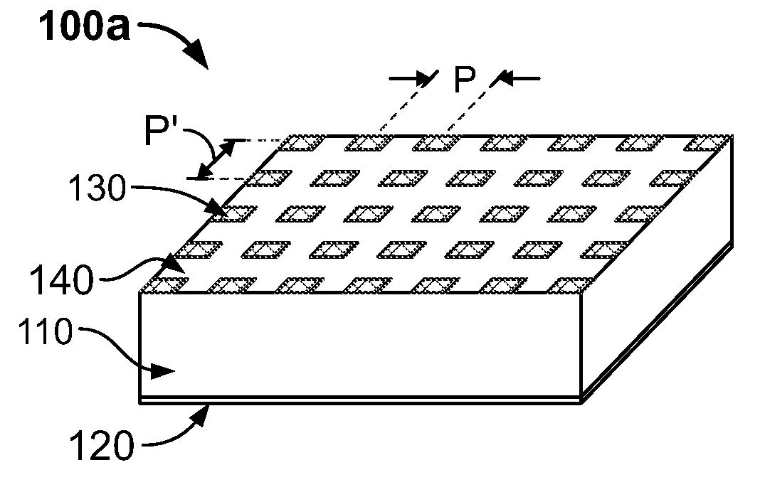
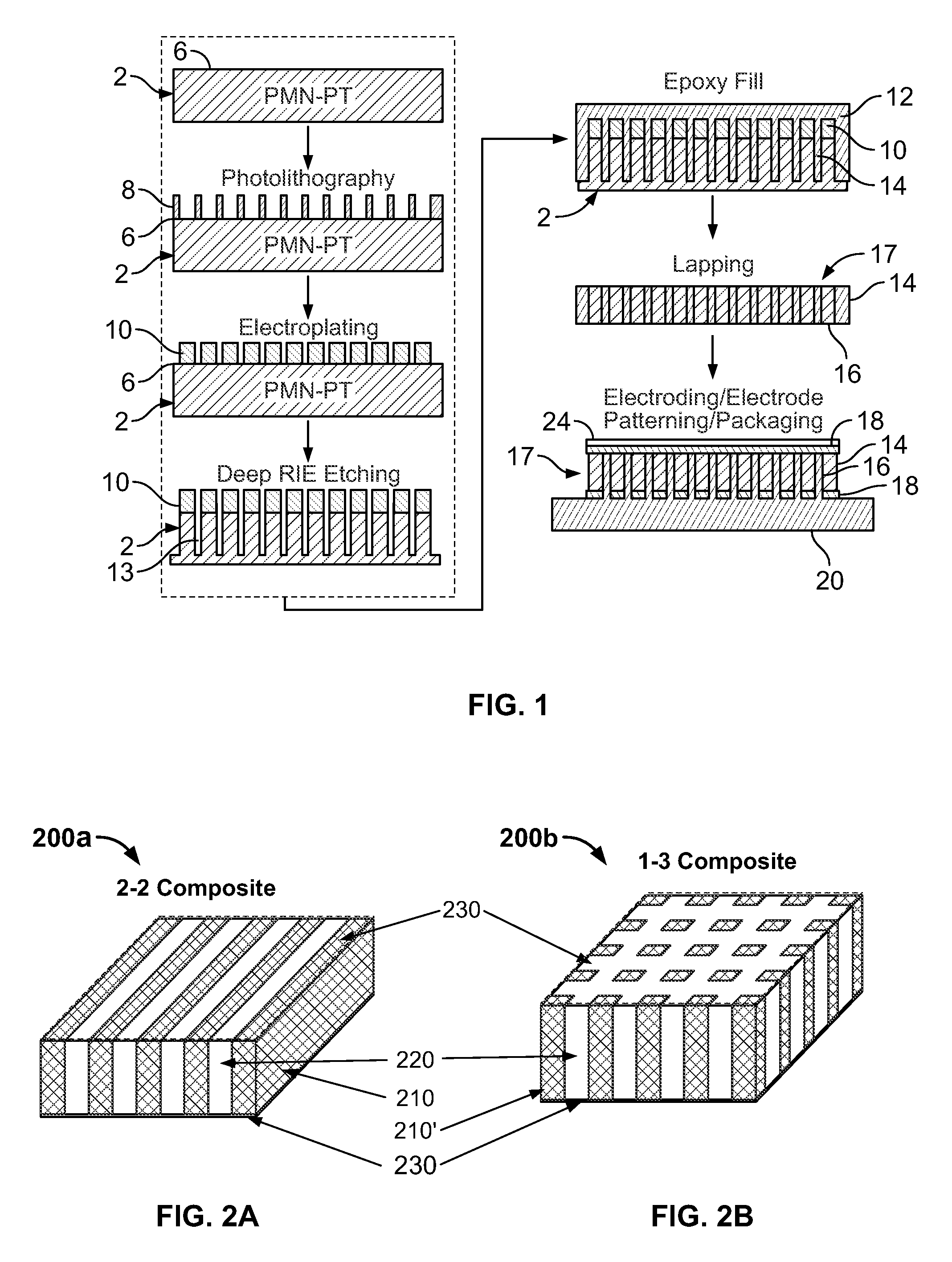
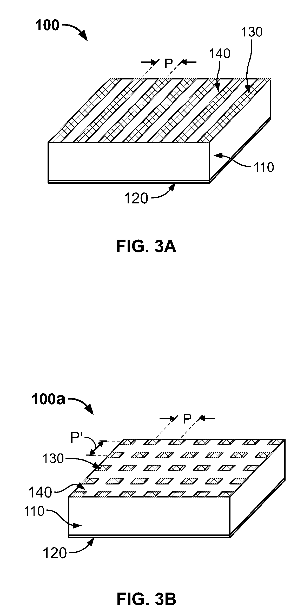
[0032]Exemplary embodiments of the invention are directed to overcoming the problems existing in the current transducer array fabrication by using photolithography-based micromachining of bulk piezoelectric materials, such as, but not limited to PZT, single crystal PMN-PT, single crystal PIN-PMN-PT, PT, and BST. The current disclosure discloses a multi-layer transducer array and a method for forming a multi-layer transducer array including deep etching to form through-wafer-vias. In one embodiment, the disclosed method can be used to form micromachined imaging transducers having a frequency range from less than 2 MHz to greater than 100 MHz. In another embodiment, the disclosed method can be used to form micromachined imaging transducers having a frequency range from about 1.5 MHz to about 300 MHz. In yet another embodiment, the disclosed method may be used to form transducers having a frequency range from about 20 MHz to about 100 MHz. The disclosed method forms transducers having ...
PUM
| Property | Measurement | Unit |
|---|---|---|
| Depth | aaaaa | aaaaa |
| Depth | aaaaa | aaaaa |
| Frequency | aaaaa | aaaaa |
Abstract
Description
Claims
Application Information
 - Generate Ideas
- Intellectual Property
- Life Sciences
- Materials
- Tech Scout
- Unparalleled Data Quality
- Higher Quality Content
- 60% Fewer Hallucinations
Browse by: Latest US Patents, China's latest patents, Technical Efficacy Thesaurus, Application Domain, Technology Topic, Popular Technical Reports.
© 2025 PatSnap. All rights reserved.Legal|Privacy policy|Modern Slavery Act Transparency Statement|Sitemap|About US| Contact US: help@patsnap.com