Cleaning method following opening etch

a cleaning method and opening etching technology, applied in the field of cleaning methods following opening etching, can solve the problems of metal residues, difficult to remove metal residues, and difficult to clean up the bond formed between silicon atoms and organic groups, and achieve the effects of improving throughput, high cleaning efficiency, and simplifying the fabrication process

Active Publication Date: 2009-06-04
UNITED MICROELECTRONICS CORP
View PDF9 Cites 47 Cited by
  • Summary
  • Abstract
  • Description
  • Claims
  • Application Information

AI Technical Summary

Benefits of technology

[0014]The present invention utilizes only an in-situ nitrogen treatment process and a wet cleaning process to achieve a high cleaning efficiency in removing the residues result from an opening etch of an interconnection fabrication; therefore, the fabrication processes can be simplified greatly so as to increase the throughput and to lower the fabrication cost. In addition, the yield can be improved substantially along with the increase of the cleaning capacity. Furthermore, because the present invention only utilizes nitrogen as a plasma source instead of using reactive gas such as hydrogen (H2), oxygen (O2), or carbon tetrafluoride (CF4), etc, as a plasma source; therefore, the problems relating to damaging low-k dielectric layers and changing the k value of the low-k dielectric layers in the prior art can be avoided.

Problems solved by technology

However, it has been found that the bond formed between the silicon atoms and the organic groups is not as stable as the silicon-oxygen bond formed in conventional silicon oxide materials.
Therefore, the bond formed between the silicon atoms and the organic groups is easily damaged during some processes of the Cu dual damascene fabrication such as an opening etch, which is performed to etch the low-k dielectric layer to form opening structures (i.e. trench or via hole), or an ashing process used for removing photoresist layers, etc.
However, the use of the hard mask layer containing metal layers as an etching mask results in metal residues, which are more difficult to remove than conventional organic photoresist layers, remaining on the bottom or the sidewall of the dual damascene structure.
However, the aforesaid cleaning methods of using H2 / O2 / CF4 plasma or only H2-containing plasma still can't remove polymers or metal residues effectively; therefore, the aim of increasing yield hasn't made a breakthrough.
As increasing in the times of wet cleaning processes, the throughput is decreased and the cost is increased.
Furthermore, the cleaning methods using reactive gases such as H2 or CH4, etc, as plasma sources usually result in damaging the low-k dielectric layer or changing the dielectric constant of the low-k dielectric layer so as to affect the capacitances of the corresponding devices.

Method used


Image

  • Cleaning method following opening etch
  • Cleaning method following opening etch
  • Cleaning method following opening etch

Examples


Embodiment Construction

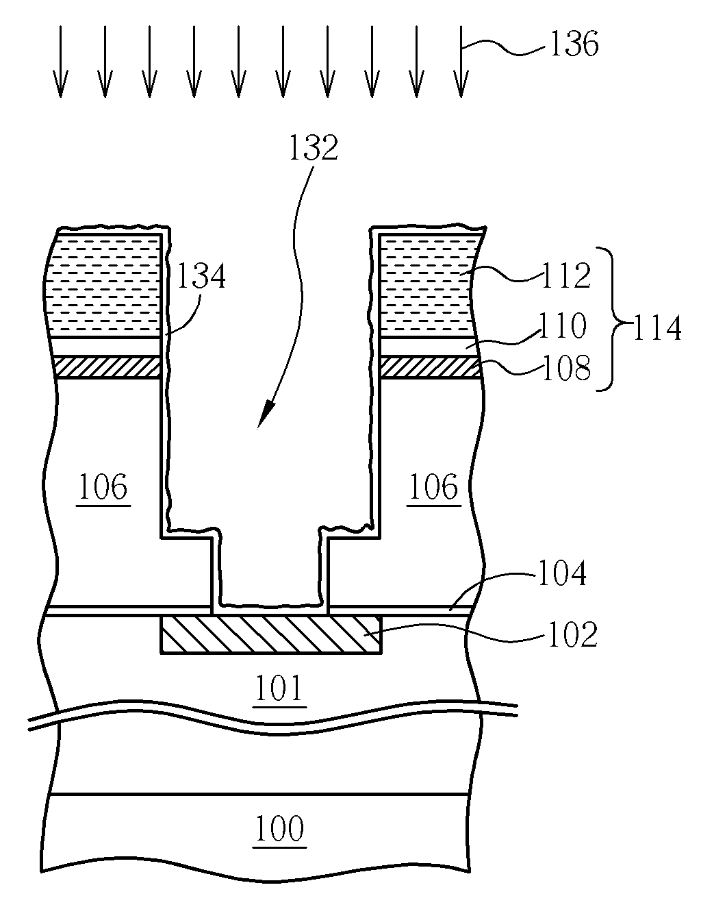
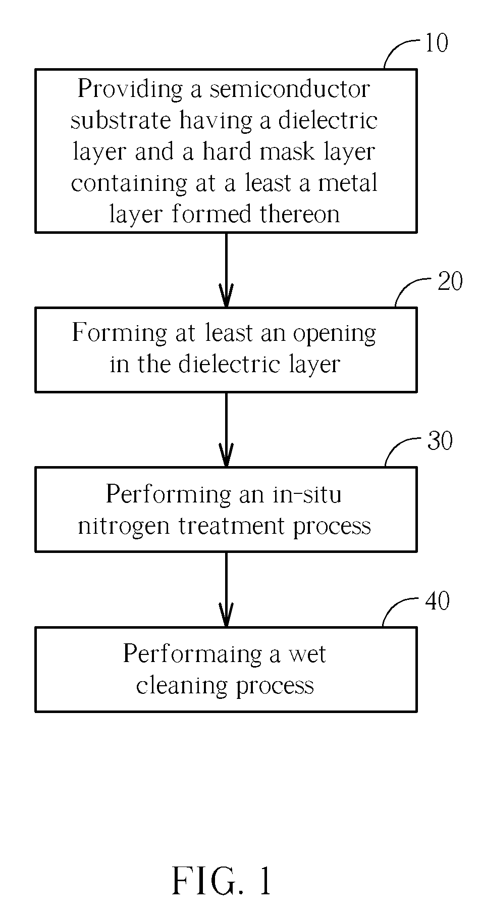
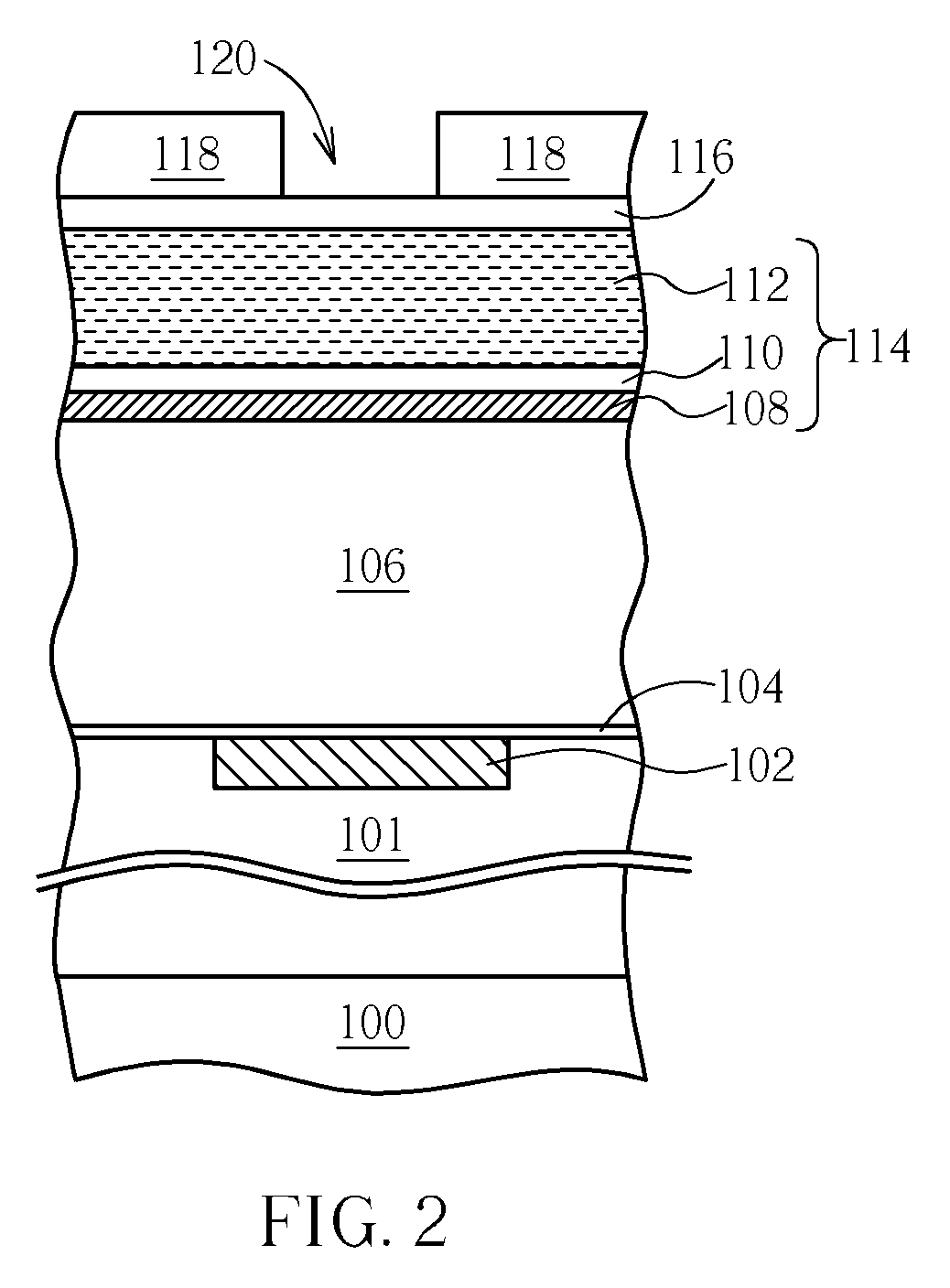
[0019]Please refer to FIG. 1, which is a flow chart of a cleaning method following an opening etch according to the present invention. As shown in FIG. 1, in step 10, at first, a semiconductor substrate such as a silicon substrate or a silicon-on-insulator (SOI) substrate, etc, is provided. A dielectric layer and a hard mask layer are formed on the semiconductor substrate. The hard mask layer comprises at least a metal layer. The semiconductor substrate may further comprise at least a functional device such as a Metal Oxide Semiconductor (MOS) transistor, etc thereon. The dielectric layer is a low-k dielectric layer such as a carbon-doped oxide (CDO) layer, an organo-silicate-glasses (OSGs) layer, a fluorinated silica glasses (FSGs) layer, or an ultra low-k (k<2.5) material layer, etc. The method of forming the low-k dielectric layer comprises a spin-coating process, a plasma-enhanced chemical vapor deposition (PECVD) process, or a high-density plasma chemical vapor deposition (HDPC...


PUM

PropertyMeasurementUnit
poweraaaaaaaaaa
reaction timeaaaaaaaaaa
dielectric constantsaaaaaaaaaa

Abstract

A cleaning method following an opening etching is provided. First, a semiconductor substrate having a dielectric layer is provided. The hard mask layer includes at least a metal layer. The opening etch is then carried out to form at least an opening in the dielectric layer. A nitrogen (N2) treatment process is performed to clean polymer residues having carbon-fluorine (C—F) bonds remained in the opening. Finally, a wet cleaning process is performed.

Description

BACKGROUND OF THE INVENTION[0001]1. Field of the Invention[0002]The present invention provides a cleaning method following an opening etch, and more particularly, to a cleaning method that utilizes an in-situ nitrogen (N2) treatment process.[0003]2. Description of the Prior Art[0004]To meet the needs of high integration and high processing speed in integrated circuits (ICs) and in semiconductor fabrication of 0.13 micrometer (μm) or below, a copper (Cu) dual damascene technology in company with low dielectric constants (k values) (low-k; k≦2.9) dielectric layer has now become an effective metal interconnection solution. The reason is because Cu has the features of lower resistance (approximately 30% lower than aluminum) and better electro-migration resistance and so on. Besides, the use of low-k materials as dielectric layers can help to reduce Resistance-Capacitance Time Delay. Therefore, low-k dielectric layer in company with Cu dual damascene in ICs fabrication has become more an...

Claims


Application Information

Patent Timeline
Patent Type & Authority Applications(United States)
IPC IPC(8): H01L21/461C23F1/12
CPCH01L21/02063H01L21/31144H01L21/76814H01L21/76813H01L21/76811
Inventor WANG, CHIEH-JUYAU, JYH-CHERNGLAI, YU-TSUNGLIAO, JIUNN-HSIUNG
Owner UNITED MICROELECTRONICS CORP
Why Eureka
Try Eureka