Apparatus and method for application of a thin barrier layer onto inner surfaces of wafer containers

Inactive Publication Date: 2009-08-20
MULTIMETRIXS
View PDF14 Cites 0 Cited by
  • Summary
  • Abstract
  • Description
  • Claims
  • Application Information

AI Technical Summary

Benefits of technology

[0022]It is an object of the present invention to provide a method and apparatus for coating the inner walls of a sealable wafer container molded from a polymer material with a thin barrier layer, such as an SiO2 layer, to prevent diffusion of free radicals of the polymer material of the container into the interior space of the container that contains the semiconductor wafers. It is another object to provide the aforementioned method and apparatus for coating the inner wal

Problems solved by technology

Contamination is the single biggest cause of yield loss in the semiconductor industry.
Despite the fact that wafer transportation and processing must be contamination free, these processes introduce organic contaminants and particles.
Such attachment and sealing requires specialized components, which may be of complex configuration.
However, wafer containers cannot completely protect wafers from particulate contamination.
However, surfaces of polymer materials are not easily washable.
Furthermore, polymeric materials are soft and easily scratchable, and the thus-formed scratches or microcracks that occur because of deformation and deterioration serve as sources of accumulated contaminants, which cannot be easily removed by washing.
When the contact area between the carrier and the wafer is large, static electricity and friction-induced formation of foreign particles occur, causing foreign particles to adhere to the wafer.
Moreover, when foreign particles adhere to a wafer, the yield in semiconductor manufacturing is also reduced.
The major cause low yield is the existence of the aforementioned contaminant particles consisting of dust, organic substances, and so forth.
Typically, a liner is destroyed after one or several uses.
Although the liner environment is as clean as possible, contaminants generated by bumping are present, as mentioned above.
Contaminants collected on the external surface of the liner cause the liner to become dirty and a potential source of contamination for subsequent processing steps when opening the SMIF box.
For example, PEEK is a material that has ideal abrasion-resistance characteristics for wafer conta

Method used


Image

  • Apparatus and method for application of a thin barrier layer onto inner surfaces of wafer containers
  • Apparatus and method for application of a thin barrier layer onto inner surfaces of wafer containers
  • Apparatus and method for application of a thin barrier layer onto inner surfaces of wafer containers

Examples


Embodiment Construction

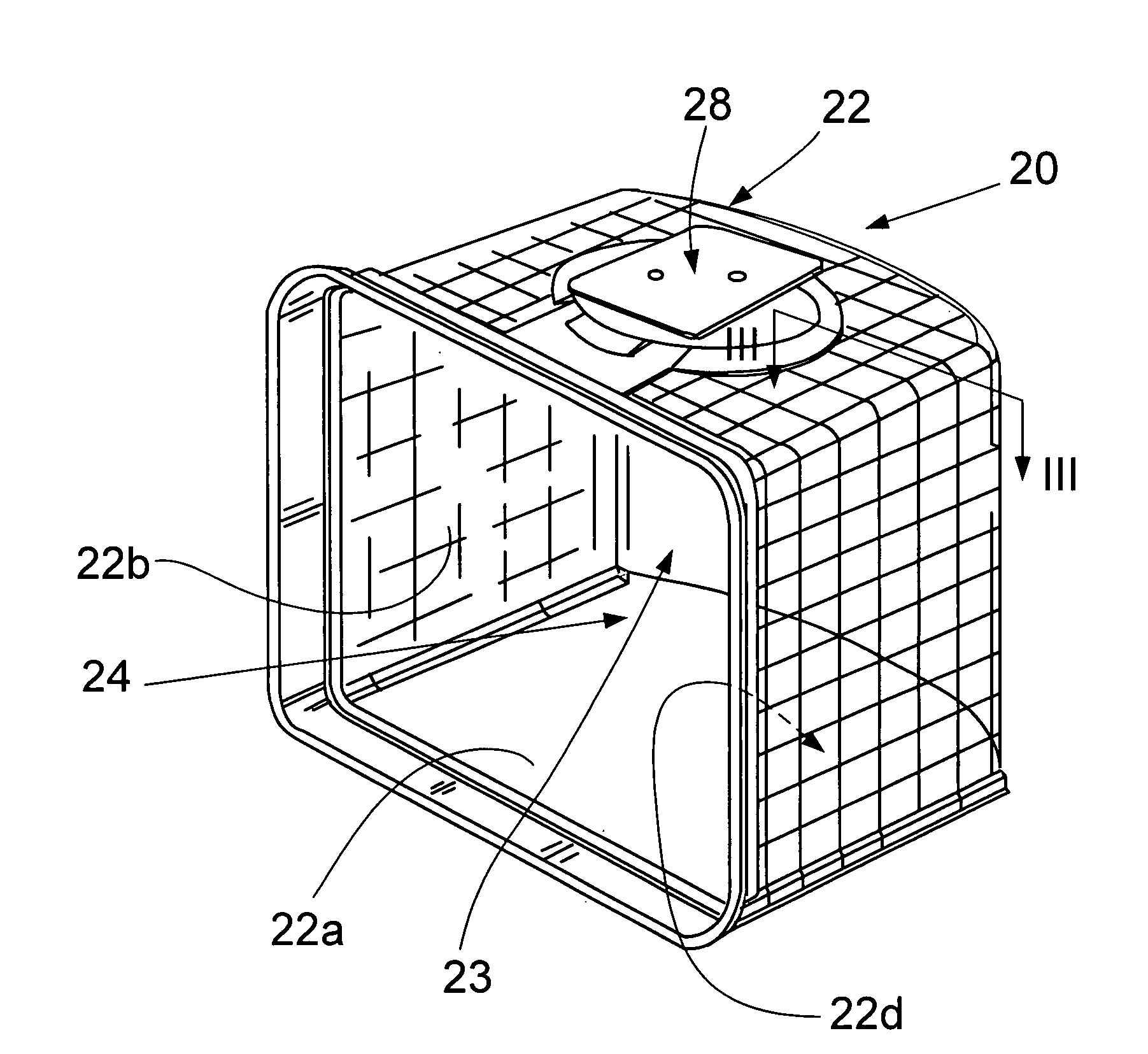
[0041]To better understand the principle of the present invention, it is advantageous first to describe the wafer containers that constitute an object of treatment with the apparatus of the invention.

[0042]Although the wafer container of the present invention may be of any suitable type, hereinafter it will be exemplified by a wafer container known as a FOUP, which typically has the shape of a box having one side open for loading and unloading wafers, manually or with the use of a mechanical arm of an industrial robot.

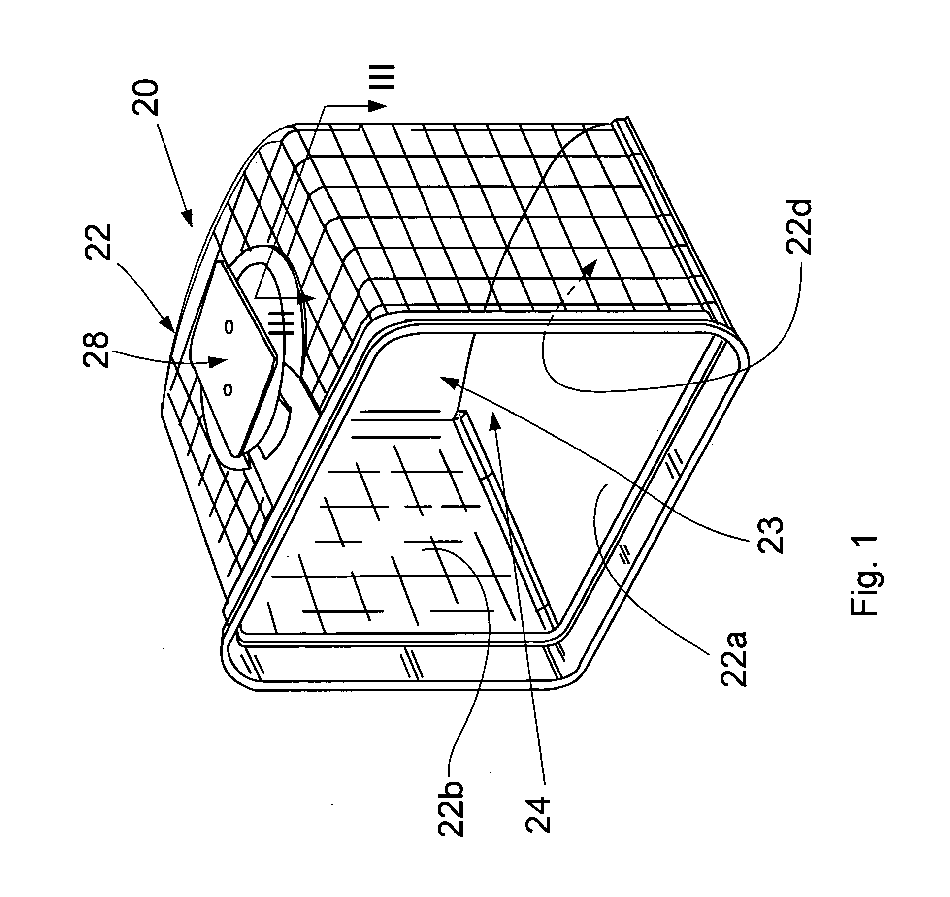
[0043]FIG. 1 is a three-dimensional view of a FOUP 20 suitable for the purposes of the present invention. The wafer containers of the type described below are beyond the scope of the present invention and constitute a subject of co-pending patent application Ser. No. ______ of the same application filed on ______

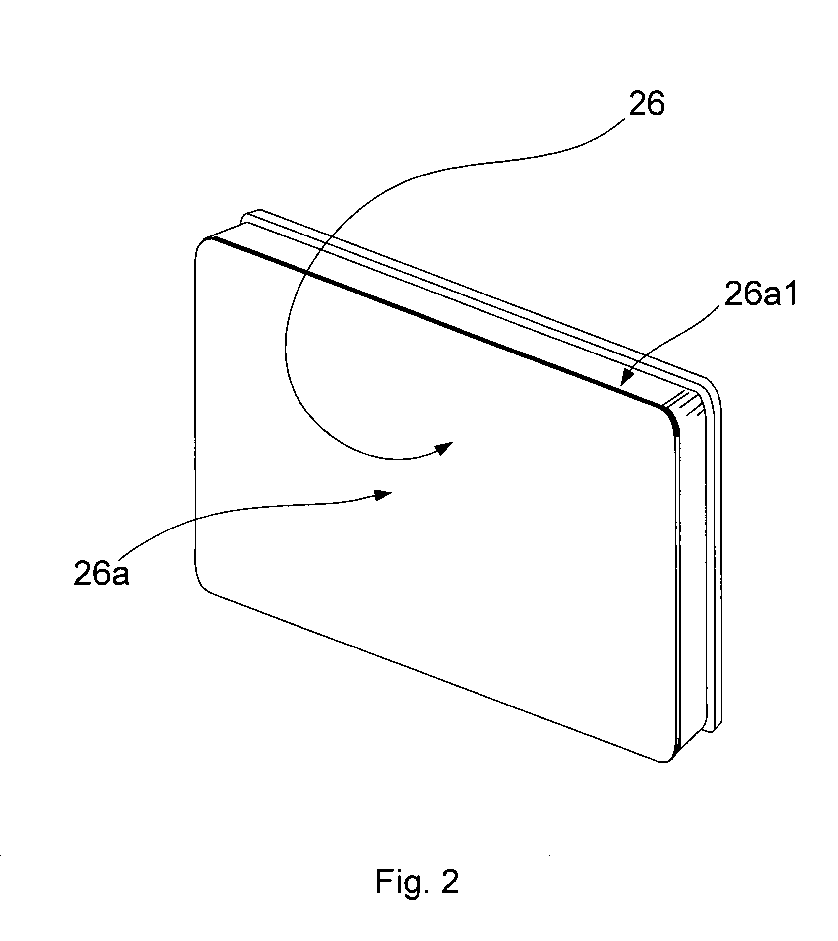
[0044]FOUP 20 is made in the form of a box 22 with an open front side 24 and with the cover removed. The cover 26 is shown in FIG. 2, which is a three-dimensio...


PUM

PropertyMeasurementUnit
Thicknessaaaaaaaaaa
Electrical conductivityaaaaaaaaaa
Electrical resistanceaaaaaaaaaa

Abstract

A method and apparatus for coating the inner walls of polymer-made wafer containers with a thin silicon dioxide barrier film, which is characterized by good washability and possesses high scratch-resistant and wear-resistant properties. In compliance with requirements of high purity, the barrier layer also protects the surfaces of semiconductor wafers from volatile substances of polymer material of the container walls. The apparatus comprises a base plate and an RF antenna unit that is inserted into the preliminarily sealed and evacuated container. The apparatus is connected to the front side of the container through a standard mechanical interface provided on the facing side of the apparatus. The barrier layer is deposited with the use of a plasma-enhanced chemical-vapor-deposition process as a result of a plasma-chemical reaction in a working gas comprising a mixture of silane with excess oxygen.

Description

FIELD OF THE INVENTION[0001]The present invention relates to the field of semiconductor production, and more particularly, to devices for storage and transportation of semiconductor wafers used for the manufacture of semiconductor devices in a mini-environment. More specifically, the invention relates to a method and apparatus for application of barrier layers onto the inner surfaces of molded and sealable wafer containers, such as FOUPs, FOSBs, etc., for improving cleanliness, washability, scratch-resistance, and wear-resistance of the inner walls of such containers. The barrier layer is made in the form of SiO2 deposited from plasma by the PECVD process with the use of an apparatus having a three-dimensional RF antenna of high conformity to the shape of interior of the container.BACKGROUND OF THE INVENTION[0002]It is well known that semiconductor processing requires operation under very clean conditions. At the present time the requirement for purity of semiconductor wafers is ver...

Claims


Application Information

Patent Timeline
IPC IPC(8): C23C16/505H05H1/24
CPCC23C16/045H01J37/321C23C16/509C23C16/402
Inventor KESIL, BORIS
Owner MULTIMETRIXS
Why Eureka
Try Eureka