Indium zinc oxide based sputtering target, method of manufacturing the same, and indium zinc oxide based thin film

a technology of zinc oxide and sputtering target, which is applied in the direction of diaphragms, metal-working apparatuses, metallic material coating processes, etc., can solve the problems of inability to use zn oxide based sputtering target in dc sputtering, limited electron mobility, and high resistivity of zn oxide based sputtering target, etc., to achieve low resistance

Inactive Publication Date: 2009-08-27
SAMSUNG CORNING PRECISION MATERIALS CO LTD
View PDF3 Cites 24 Cited by
  • Summary
  • Abstract
  • Description
  • Claims
  • Application Information

AI Technical Summary

Benefits of technology

[0008]An aspect of the present invention provides an indium (In) zinc (Zn) oxide based sputtering target having a low resistance.

Problems solved by technology

However, in a case of the polycrystalline silicon film, electron mobility may be limited due to dispersion of electrons occurring in a polycrystalline particle interface.
However, in a case of a Zn oxide based sputtering target used for depositing the Zn oxide based thin film, a resistivity of the Zn oxide based sputtering target may be significantly high depending on a type and amount of a material to be doped, whereby it is impossible for the Zn oxide based sputtering target to be used in the DC sputtering.

Method used


Image

  • Indium zinc oxide based sputtering target, method of manufacturing the same, and indium zinc oxide based thin film
  • Indium zinc oxide based sputtering target, method of manufacturing the same, and indium zinc oxide based thin film
  • Indium zinc oxide based sputtering target, method of manufacturing the same, and indium zinc oxide based thin film

Examples


example 1

HIZO (Hafnium Indium Zinc Oxide) Sputtering Target Manufacturing

[0046]A Hf oxide power, an In oxide power, and a Zn oxide power each having an average diameter of about 1 μm or less were prepared so that a ratio of Hf:In:Zn was about 1:0.4:0.4. Next, the prepared oxide powders were respectively mixed in a mixture in which water and a polycarbonic acid-ammonium salt are mixed, and each of the mixtures was wet-milled for about one hour using a hard zirconia-ball mill. Next, the wet-milled mixtures were mixed to prepare a slurry mixture. Next, the polycarbonic acid-ammonium salt was added in the slurry mixture, wet-milled for about one hour using the hard zirconia-ball mill, and then polyvinyl alcohol (PVA) was added. Next, the slurry mixture with the PVA added therein was formed into a dried granular powder using a spray dryer. Next, the granular powder was first-pressed with a pressure of about 500 kg / cm2 using a cold press method, and the first-pressed granular powder was second-pre...

example 2

HIZO Thin Film Manufacturing

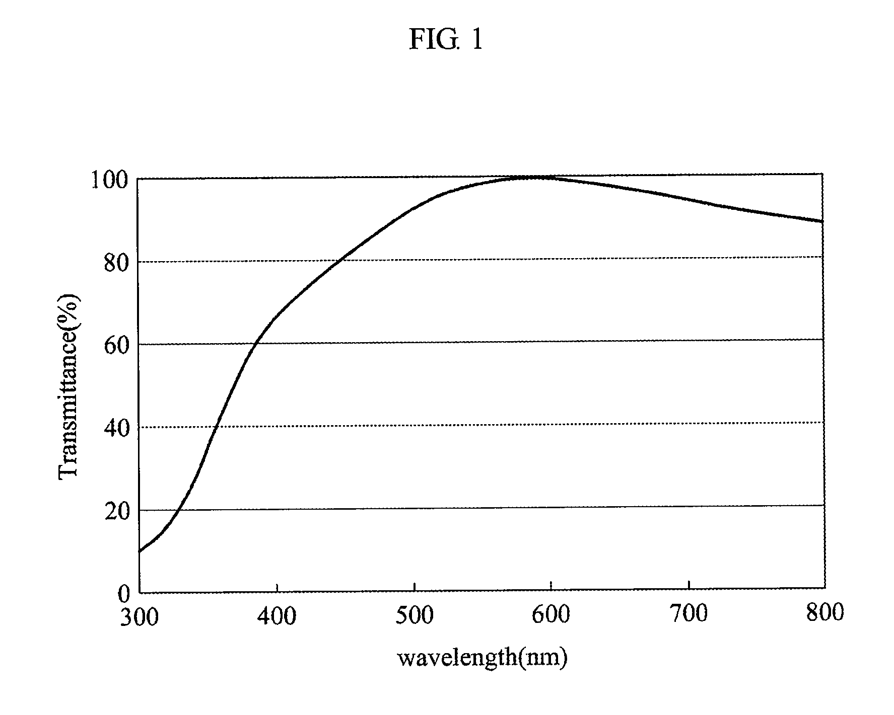
[0047]The HIZO sputtering target manufactured through Example 1 was mounted on a magnetron sputtering device, and an oxygen and argon gas were injected at room temperature to deposit a transparent HIZO thin film having a thickness of about 150 nm on a glass substrate. In this instance, the HIZO thin film was deposited under a mixed gas atmosphere of the argon gas and the oxygen gas in which a volume of the oxygen gas was about 15%. In addition, a DC power was about 100 W In this instance, in the DC power of about 100 W, the HIZO thin film was deposited at a deposition speed (11 Å / sec) faster than a deposition speed (9 Å / sec) of a conventional Gallium Indium Zinc Oxide (GIZO).

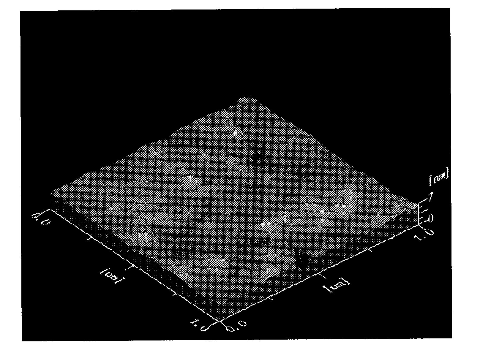
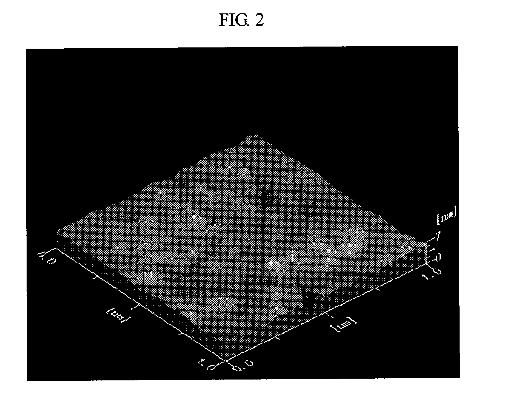
[0048]The HIZO thin film manufactured through Example 2 was analyzed using X-ray diffraction (XRD), and as a result, the HIZO thin film exhibited amorphous characteristics. An electrical conductivity of the HIZO thin film was measured, and as a result, a range value of 1 E−4 to 3 E−3 ...


PUM

PropertyMeasurementUnit
electron mobilityaaaaaaaaaa
temperatureaaaaaaaaaa
sizeaaaaaaaaaa

Abstract

Disclosed are an indium (In) zinc (Zn) oxide based sputtering target, a method of manufacturing the same, and an In Zn oxide based thin film deposited using the In Zn oxide based sputtering target. The In Zn oxide based sputtering target has a composition of (MO2)x(In2O3)y(ZnO)z, in which x:y is about 1:0.01 to 1:1, y:z is about 1:0.1 to 1:10, and M is at least one metal selected from a group consisting of hafnium (Hf), zirconium (Zr), and titanium (Ti).

Description

CROSS-REFERENCE TO RELATED APPLICATION[0001]This application claims the benefit of Korean Patent Application No. 10-2008-0017513, filed on Feb. 26, 2008 in the Korean Intellectual Property Office, the disclosure of which is incorporated herein by reference.BACKGROUND[0002]1. Field of the Invention[0003]The present invention relates to manufacturing of a sputtering target and manufacturing of a thin film using the sputtering target, and more particularly, to an indium (In) zinc (Zn) oxide based sputtering target, a method of manufacturing the same, and an In Zn oxide based thin film deposited using the In Zn oxide based sputtering target.[0004]2. Description of the Related Art[0005]A thin film transistor (TFT) may be a small-sized multiplier tube shaped into a fine and thin film, and may be a three-terminal device including a gate, a source, and a drain. In a conventional art, a polycrystalline silicon film or an amorphous silicon film may be generally used as a channel layer of the ...

Claims


Application Information

Patent Timeline
Patent Type & Authority Applications(United States)
IPC IPC(8): C23C14/00B29C43/02
CPCC23C14/3414C23C14/08B22F3/10B22F1/05
Inventor LEE, YOON-GYULEE, JIN-HOYOU, YIL-HWANPARK, JU-OK
Owner SAMSUNG CORNING PRECISION MATERIALS CO LTD
Why Eureka
Try Eureka