Compositions and methods for selective removal of metal or metal alloy after metal silicide formation

a technology of metal silicide and composition, which is applied in the field of composition and methods for selective removal of metal or metal alloy after metal silicide formation, can solve the problems of increased resistance at the interface, damage to the substrate surface, and difficulty in further minimizing the size of the source/drain region

Inactive Publication Date: 2009-08-27
ADVANCED TECH MATERIALS INC
View PDF52 Cites 60 Cited by
  • Summary
  • Abstract
  • Description
  • Claims
  • Application Information

AI Technical Summary

Benefits of technology

[0018]In another aspect, the present invention relates to an aqueous metal etching composition that comprises oxalic acid, a chloride-containing compound, and optionally hydrogen peroxide, which is effective for removal of unreacted nickel, cobalt, and / or alloy thereof after formation of nickel silicide and / or cobalt silicide.
[0019]In still another aspect, the present invention relates to an aqueous metal etching composition that includes oxalic acid, a chloride-containing compound, hydrogen peroxide, borofluoric acid, and boric acid, which is particularly effective for removal of nickel, cobalt, titanium, tungsten and / or alloys thereof after silicide formation, without attacking the dielectric material and / or the semiconductor substrate.
[0020]In still another aspect, the present invention relates to an aqueous metal etching composition that includes oxalic acid, a chloride-containing compound, borofluoric acid, optionally hydrogen peroxide, and optionally boric acid, which is particularly effective for removal of nickel silicide, cobalt silicide, and titanium nitride, without attacking the dielectric material and / or the semiconductor substrate.

Problems solved by technology

A problem associated with this metallization process is that the contact may be misaligned with the gate electrode and source / drain regions, resulting in increased resistance at the interface.
Furthermore, aligning contact windows via a separate masking step makes it difficult to further minimize the size of the source / drain regions.
Plasma etching often results in damage to the substrate surface and leaves residual trace ionic contamination.
Chemical etching, on the other hand, results in less substrate damage, but the nickel etching rates using conventional chemical etchants are either very slow or not compatible with the MOS device fabrication process.

Method used


Image

  • Compositions and methods for selective removal of metal or metal alloy after metal silicide formation
  • Compositions and methods for selective removal of metal or metal alloy after metal silicide formation

Examples


example 1

[0080]Compositions 1-15 were made up according to the formulations in Table 2 below, wherein the percentages of the respective ingredients are by weight, based on the total weight of the composition, and wherein the weight percentages of all ingredients total to 100 weight percent.

TABLE 2CompositionHBF4H3BO3Oxalic AcidHClH2OH2O21004.8%0.75%Balance12%20.48%2.40%31.20%40.60%50.30%60.12%70.05%81.20%2.40%91.20%100.60%110.30%120.12%130.05%142.40%2.40%151.20%

[0081]The compositions were evaluated as etchants for various substrates including titanium nitride (TiN), polysilicon (Poly Si), thermal oxide dielectric material (TOX), tetraethylorthosilicate (TEOS), silicon nitride (SiN) and nickel silicide (NiSi). Each of the substrates was processed at 40° C. for 15 minutes and etch rates were determined in Angstroms per minute (Å / minute). Etch rates for all Compositions 1-15 were >5000 Å / minute on cobalt metal, and were >4000 Å / minute on nickel metal. Table 3 below shows the etch rate data.

TABL...

example 2

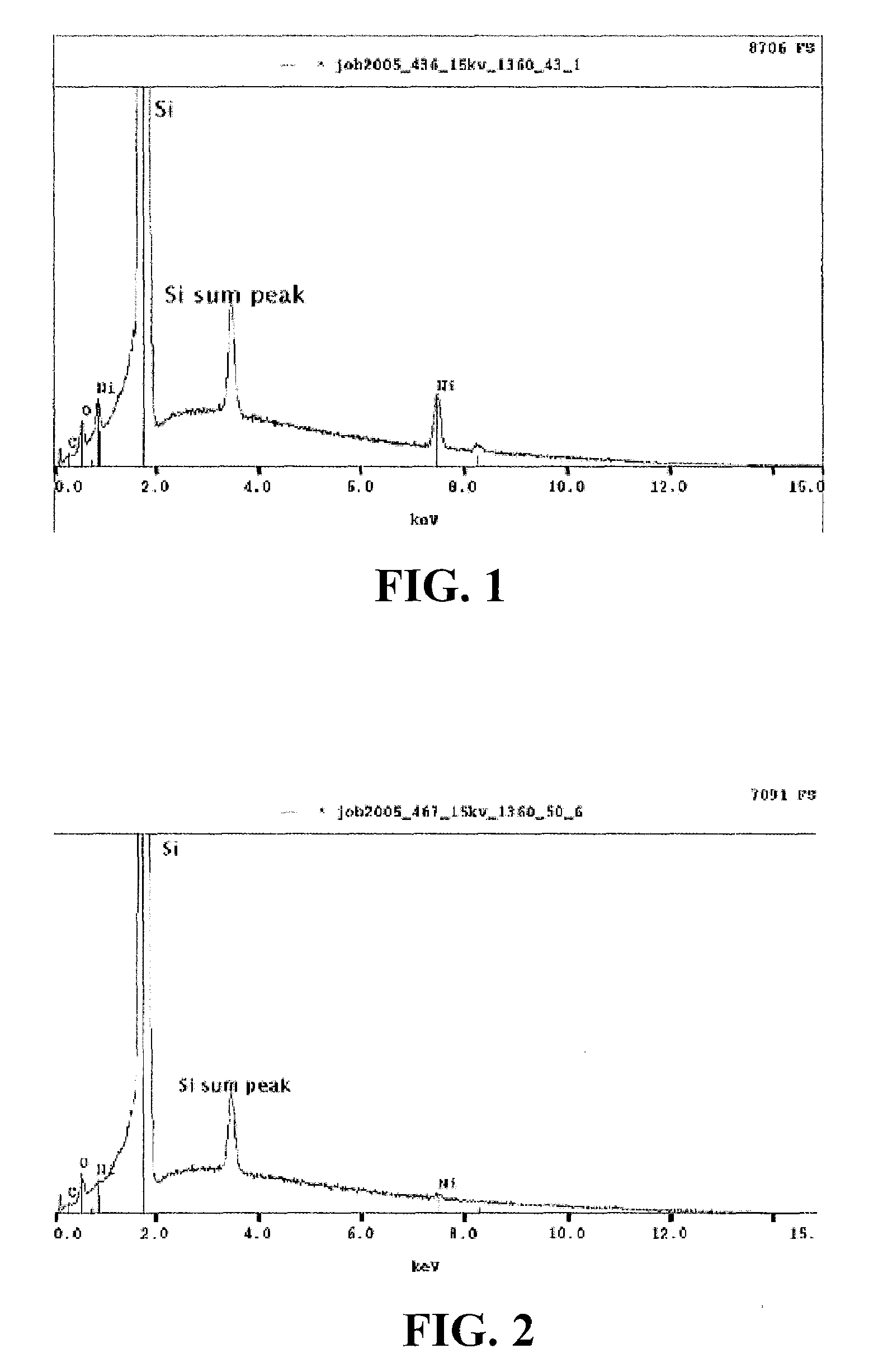
[0083]Energy dispersive x-ray spectroscopy studies were conducted on a silicon substrate having a film of nickel silicide thereon at a thickness of approximately 255 Angstroms.

[0084]FIG. 1 is an energy dispersive x-ray spectroscopy graph for a control sample of the silicon substrate having a NiSi film thereon. Significant nickel peaks are present in the graph.

[0085]FIG. 2 is an energy dispersive x-ray spectroscopy graph for the NiSi film on silicon substrate sample, as processed with Composition 7 of Example 1 for 15 minutes at 40° C. In comparison with the graph of FIG. 1, the nickel peaks are substantially absent in the graph of FIG. 2, indicating that the NiSi film (˜255 Angstroms) has been etched away. Scanning electron microscopy (SEM) was conducted on the sample, and provided cross-sectional images that also confirmed that the NiSi layer had been removed by the etching composition.

example 3

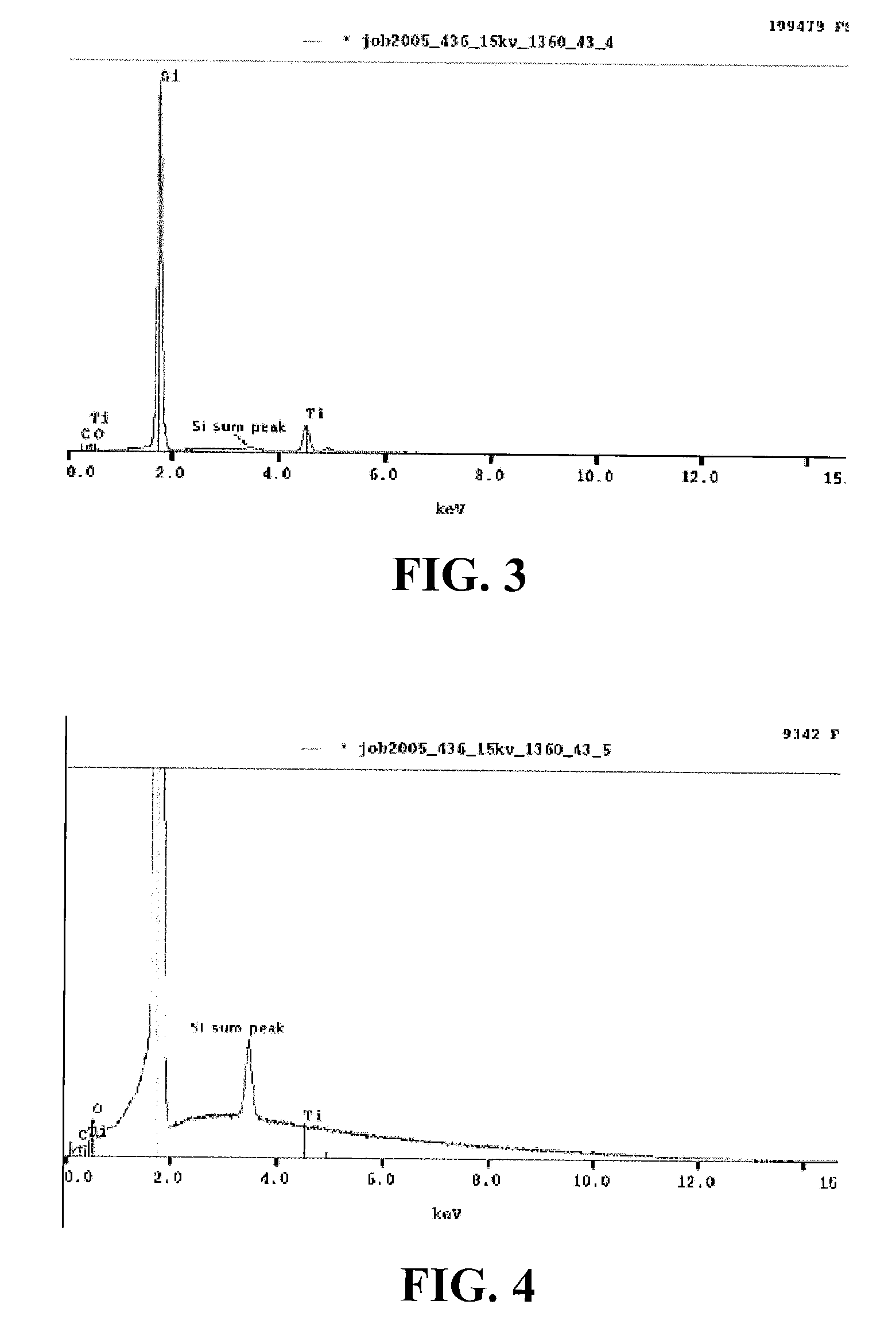
[0086]Energy dispersive x-ray spectroscopy studies were conducted on a silicon substrate having a film of titanium nitride thereon at a thickness of approximately 1,000 Angstroms.

[0087]FIG. 3 is an energy dispersive x-ray spectroscopy graph for a control sample of the silicon substrate having a TiN film thereon. A significant titanium peak is observed.

[0088]FIG. 4 is an energy dispersive x-ray spectroscopy graph for the TiN film on silicon substrate sample, as processed with Composition 14 of Example 1 for 15 minutes at 60° C. In comparison with the graph of FIG. 3, the titanium peak is substantially absent in the graph of FIG. 4, indicating that the TiN film (˜1000 Angstroms) has been etched away. Scanning electron microscopy (SEM) was conducted on the sample, and provided cross-sectional images that also confirmed that the TiN layer had been removed by the etching composition.


PUM

PropertyMeasurementUnit
temperaturesaaaaaaaaaa

Abstract

An aqueous metal etching composition useful for removal of metals such as nickel, cobalt, titanium, tungsten, and alloys thereof, after formation of metal silicides via rapid thermal annealing during complementary metal-oxide-semiconductor (CMOS) transistor fabrication. The aqueous metal etching composition is also useful for selective removal of metal silicides and/or metal nitrides for wafer re-work. In one formulation, the aqueous metal etching composition contains oxalic acid, and a chloride-containing compound, and in other formulations, the composition contains an oxidizer, such as hydrogen peroxide, and a fluoride source, e.g., borofluoric acid. The composition in another specific formulation contains borofluoric acid and boric acid for effective etching of nickel, cobalt, titanium, tungsten, metal alloys, metal silicides and metal nitrides, without attacking the dielectric and the substrate.

Description

FIELD OF THE INVENTION[0001]The present invention relates to compositions and methods for removal of unreacted metal or metal alloy after metal silicide formation during a microelectronic device fabrication process. In addition, the present invention relates to compositions and methods for selective removal of metals, metal compounds and / or metal alloys used in microelectronic device fabrication for wafer re-work.DESCRIPTION OF THE RELATED ART[0002]Over the last few decades, the semiconductor industry has undergone a revolution in the use of silicon-based technology to fabricate small, highly integrated electronic devices. One silicon-based microelectronic device is a metal-oxide-semiconductor (MOS) transistor, which is one of the basic building blocks of modern personal computers.[0003]The process of forming of contacts to the gate electrode and source / drain regions of the MOS transistors is generally referred to as “metallization.” The term metallization is generic in its applicat...

Claims


Application Information

Patent Timeline
Patent Type & Authority Applications(United States)
IPC IPC(8): B44C1/22C09K13/00C09K13/06C09K13/08
CPCC23F1/28C23F1/26H01L21/32134C23F1/02C23F1/30C23F1/16C09K13/08
Inventor BERNHARD, DAVID D.WANG, WEIHUABAUM, THOMAS H.
Owner ADVANCED TECH MATERIALS INC
Why Eureka
Try Eureka