

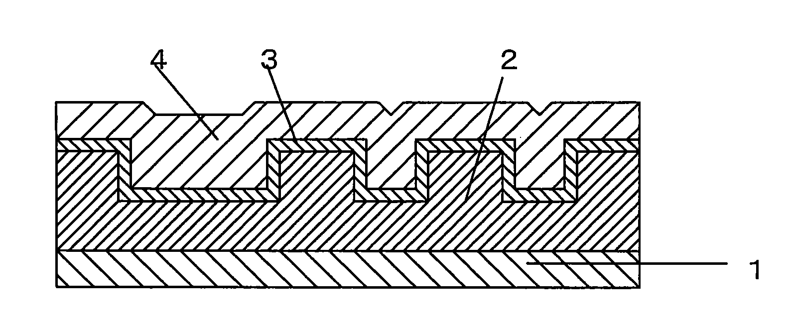
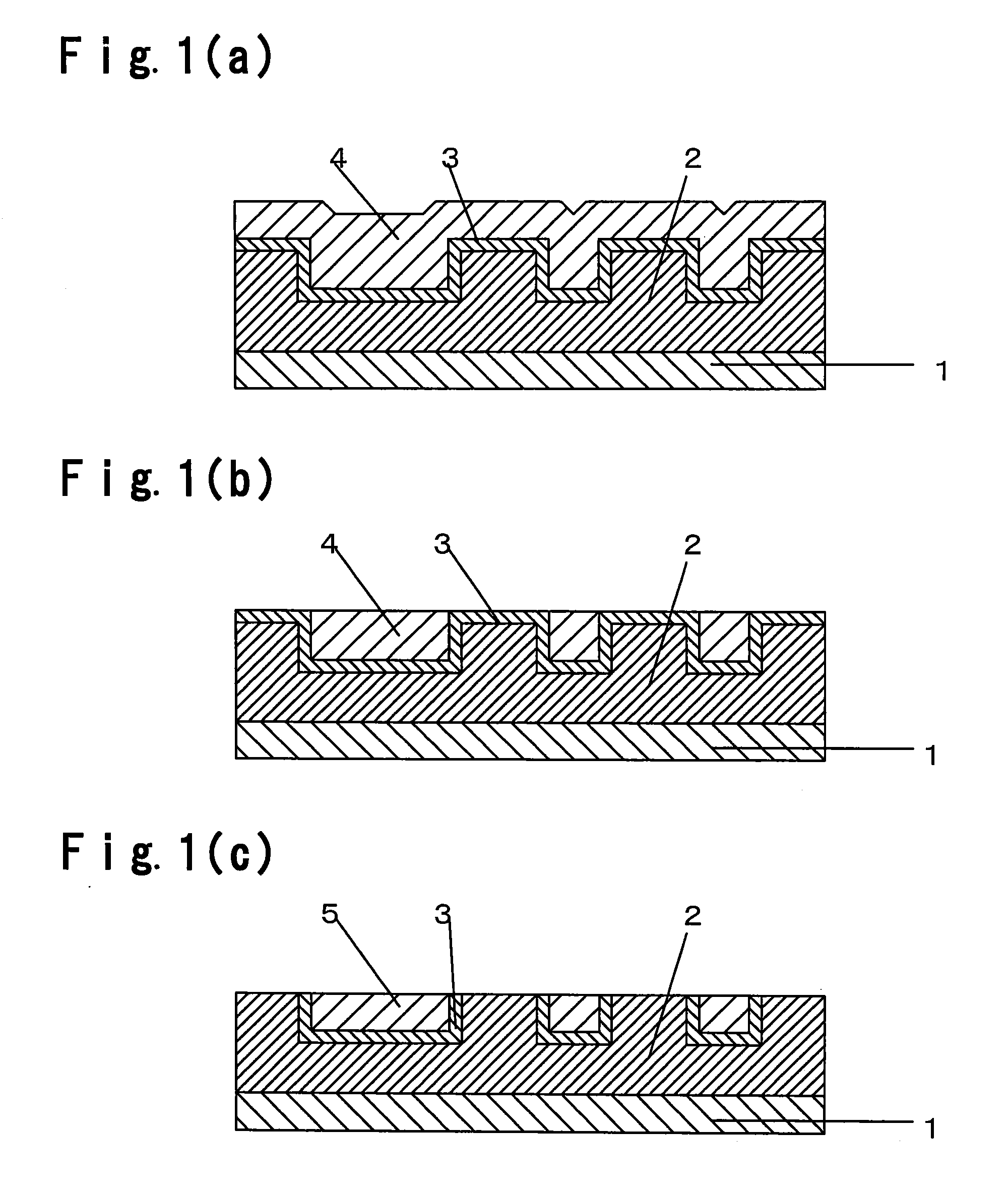
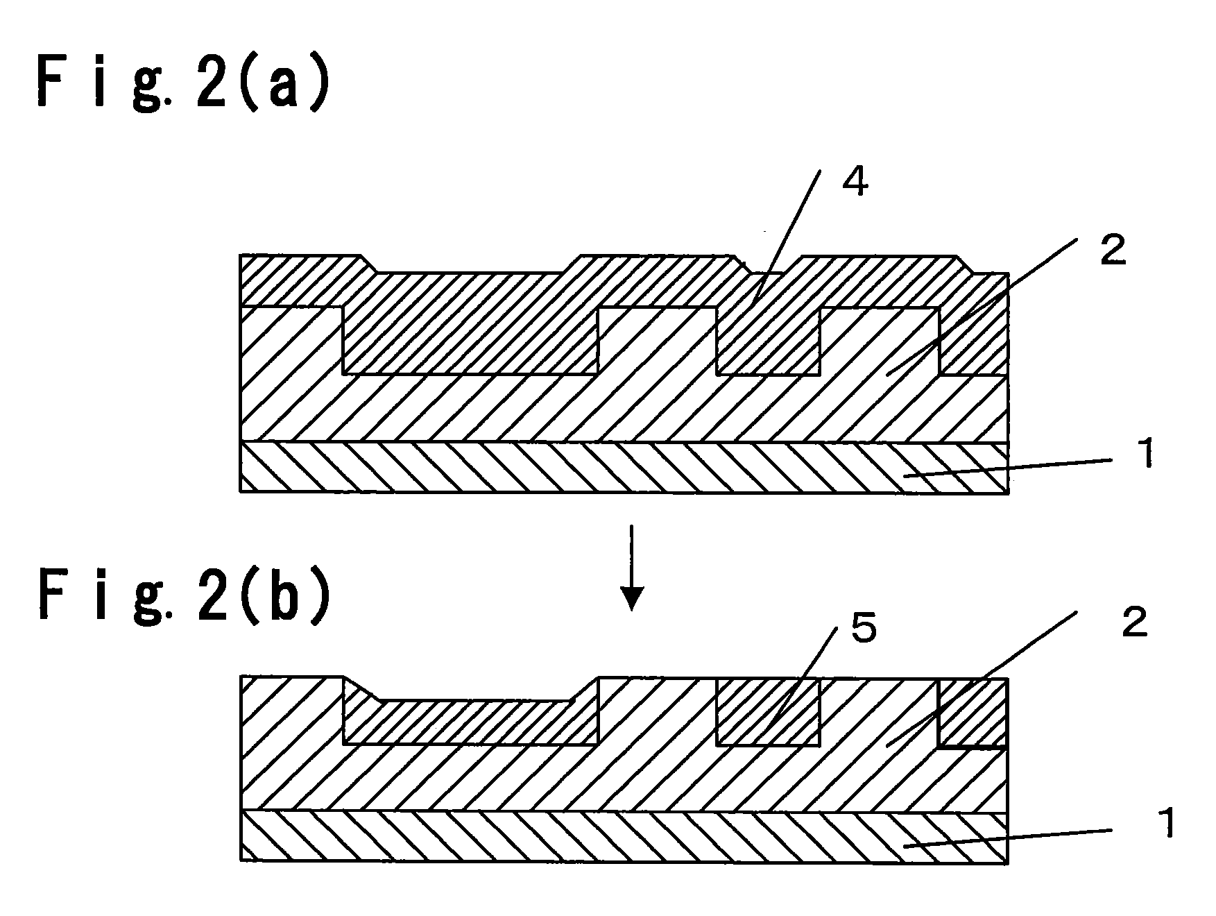
Polishing compound, its production process and polishing method
a technology of polishing compound and polishing method, which is applied in the field of polishing compound, can solve the problems of difficult to form copper into the shape of wirings, difficulty in forming copper into wirings, and differences in level that exceed the depth of focus in lithography, and achieve the effect of suppressing wiring defects and high removal ra
- Summary
- Abstract
- Description
- Claims
- Application Information
AI Technical Summary
Benefits of technology
Problems solved by technology
Method used
Image

Examples
examples 1 to 3
[0060]Using a polishing compound having a composition as shown in Table 1, polishing was carried out on a wafer for evaluating removal rate of copper and the patterned wafer. The numerals in Table 1 represent the proportion by mass of the respective components to the total mass of the polishing compound, and the unit is %.
[0061]The polishing conditions were as described below, and the removal rate when the wafer for evaluating removal rate of copper was polished with each polishing compound, was measured by using a film thickness measuring apparatus (RT80-RG80, manufactured by Napson Corporation). Further, with respect to polishing of the patterned wafer, dishing at a position with the line width of 50 μm was measured by using a profilometer (Dektak V200Si manufactured by Veeco Instruments). The results are shown in Table 2. In Table 2, the unit of the removal rate is nm / min, and the unit of dishing is nm.
(Polishing Conditions)
examples 4 to 6
[0068]Using each polishing compound having a composition as shown in Table 1, polishing was carried out on the patterned wafer. In Examples 4 and 5, polishing was carried out also on the wafer for evaluating removal rate of copper, and in Examples 4 and 6, polishing was carried out also on the wafer for evaluating removal rate of tantalum, and the removal rate of copper and the removal rate of tantalum were compared.
[0069]The polishing conditions were as described below, and the removal rates when the wafer for evaluating removal rate of copper and the wafer for evaluating removal rate of tantalum were polished were measured by using a film thickness measuring apparatus (tencor RS-75 manufactured by KLA-Tencor Corporation). Further, with respect to the polishing of the patterned wafer, dishing at a position with the line width of 50 μm was measured by using a profilometer (tencor HRP-100 manufactured by KLA-Tencor Corporation). The results are shown in Table 2.
(Polishing Conditions)...
examples 7 and 8
[0075]Using each polishing compound having a composition as shown in Table 1, polishing was carried out on the wafer for evaluating removal rate of copper and the wafer for evaluating removal rate of tantalum in the same manner as in Example 4. Polishing was carried out in the same manner as in Example 4 except that the polishing compound supply amount was changed to 100 mL / min. The results are shown in Table 2.
TABLE 1Ex. 1Ex. 2Ex. 3Ex. 4Ex. 5Ex. 6Ex. 7Ex. 8δ-alumina2.772.772.772.772.772.770.950.95Tartaric acid0.920.9200.9200.920.950.95Malonic acid0.9201.850.921.850.920.950.95Maleic acid00.9200.920000BTA0.0460.0460.0460.00900.0090.0290.010THMAM3.693.693.693.693.6901.903.81Ammonia000000.460.240H2O22.312.312.312.312.312.311.431.43WaterthethethethethethethetherestrestrestrestrestrestrestrestpH6.56.56.56.56.56.577
TABLE 2Ex. 1Ex. 2Ex. 3Ex. 4Ex. 5Ex. 6Ex. 7Ex. 8Copper8387951034578527381929696removal rateTa removal rate———0.5— 333.31.7Dishing100100 19055130———
PUM
| Property | Measurement | Unit |
|---|---|---|
| mass % | aaaaa | aaaaa |
| mass % | aaaaa | aaaaa |
| mass % | aaaaa | aaaaa |
Abstract
Description
Claims
Application Information