Conductive pattern forming film, and conductive pattern forming method and conductive pattern forming apparatus for the conductive pattern forming film

a technology of conductive pattern and forming method, which is applied in the direction of dough shaping, manufacturing tools, applications, etc., can solve the problems of difficult to implement printed devices on plastic films, difficult to reduce process costs, and negative impact on the environment, and achieves easy formation of highly electrically conductive patterns, simple operation, and simple structure

Inactive Publication Date: 2010-02-04
NAT INST OF ADVANCED IND SCI & TECH
View PDF15 Cites 15 Cited by
  • Summary
  • Abstract
  • Description
  • Claims
  • Application Information

AI Technical Summary

Benefits of technology

[0037]According to the present invention, by using a manufacturing apparatus of simple structure, a conductive pattern can be formed on a substrate at low temperature with a simple operation with ease.
[0038]Even when a general conductive printing ink is used, a wiring pattern of high electrical conductivity or high-performance thin semiconductor film can still be formed on a flexible substrate at low temperature.
[0039]Also, a conductive pattern forming film as well as a method for forming conductive pattern and a conductive pattern forming apparatus for the same, all according to the present invention, allow for easy formation of a highly electrically conductive pattern by using an apparatus that implements a simple pressurization process at low temperature, in order to form conductive patterns in large volumes at low cost on general plastic substrates having flexibility.
[0040]Since it uses a low-temperature baking technology involving 150° C or below, the present invention can also be applied to plastics whose processing temperature is relatively low.
[0041]In addition, the present invention is also applicable to semiconductor pastes, which means that an active element can be formed on a film having flexibility using a low-temperature coating process.
[0042]According to the present invention, it is also possible to form, on a film having flexibility, metal electrodes having various work functions. Accordingly, the present invention can be applied to flexible batteries, electro-chromic display elements, electro-luminescence elements, diode elements, etc.

Problems solved by technology

However, a vacuum environment is an essential requirement of the heat deposition method and sputtering method, and thus reducing the process cost has been difficult.
Also, the photo-lithography method requires a large amount of solvent, which is pointed out as a negative impact on the environment.
On the other hand, many flexible plastic films soften and melt at high temperatures, and it is therefore difficult to implement printed devices on plastic films.
However, metal nano-particles are expensive and therefore it is difficult, with metal nano-particles, to achieve the purpose of manufacturing products in large volumes at low cost.

Method used


Image

  • Conductive pattern forming film, and conductive pattern forming method and conductive pattern forming apparatus for the conductive pattern forming film
  • Conductive pattern forming film, and conductive pattern forming method and conductive pattern forming apparatus for the conductive pattern forming film
  • Conductive pattern forming film, and conductive pattern forming method and conductive pattern forming apparatus for the conductive pattern forming film

Examples


example 1

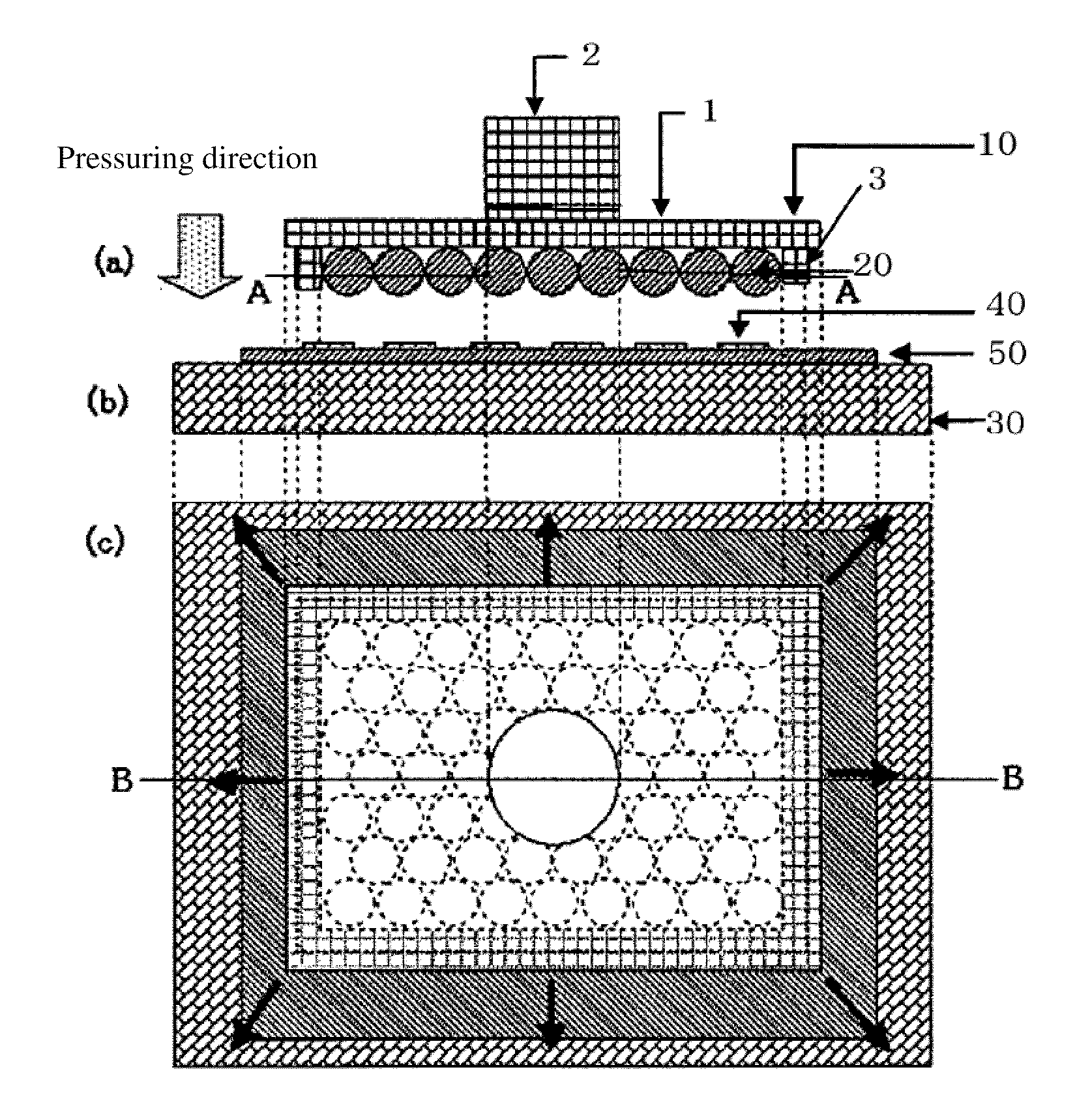
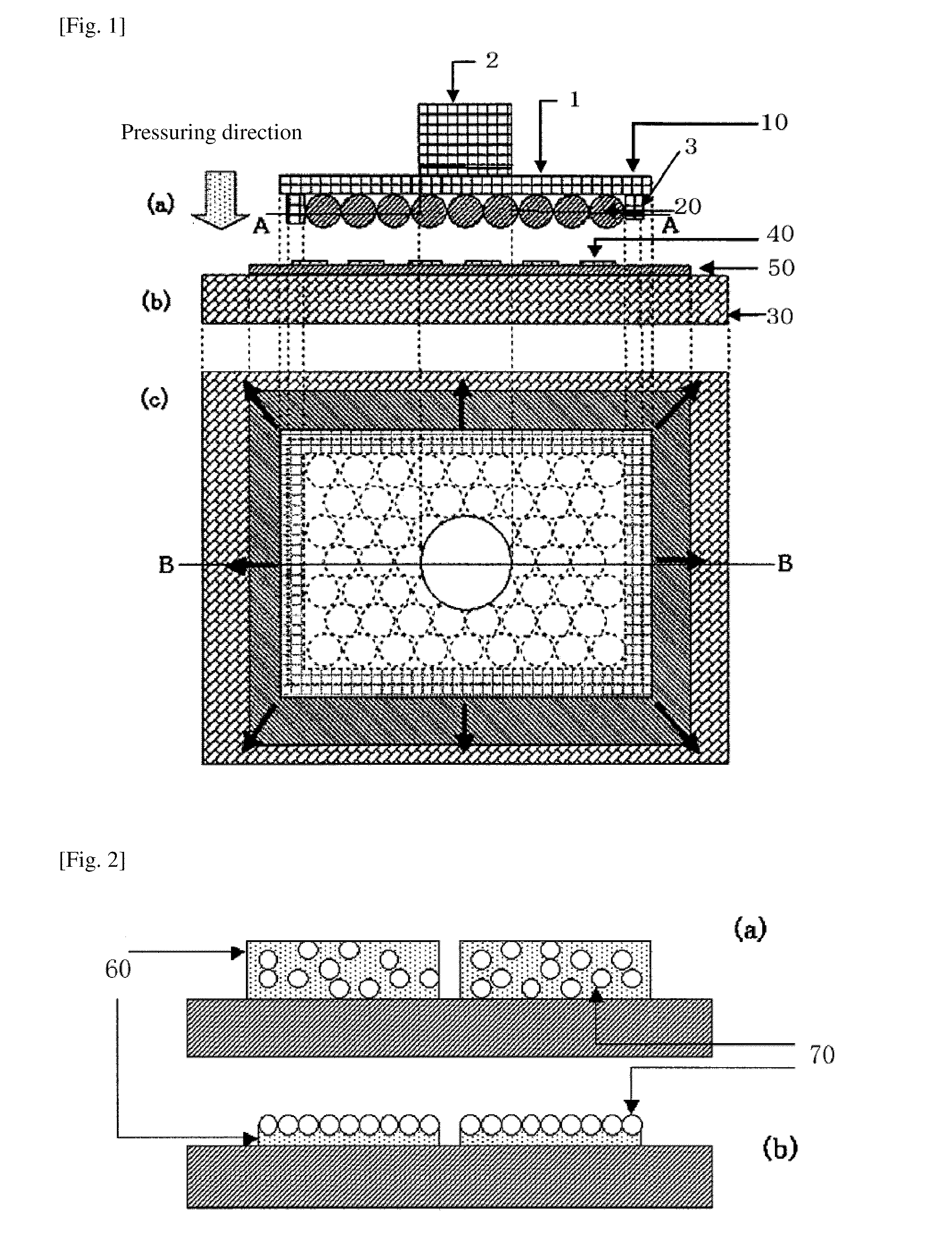
[0126]A conductive pattern forming apparatus according to the present invention comprises a driving body for pressure application 10 and a sample installation table 30, as shown in FIG. 1. In FIG. 1, FIG. 1(a) is a section view of the driving body for pressure application (section B-B of FIG. 1(c)), FIG. 1(b) is a section view of the sample installation table (section B-B of FIG. 1(c)), and FIG. 1(c) is a top view of section A-A of FIG. 1(a) when the section is rotated around the center axis. The driving body for pressure application 10 is structured in such a way that it has a column-shaped magnet 2 on the top face of a flat metal plate 1, and a rectangular frame 3 is provided below this flat metal plate 1, with a plurality of metal spheres 20 arranged, without any gap left in between, in a single row along the bottom face of the flat metal plate 1 inside this rectangular frame 3. The metal spheres 20 are attracted to the flat metal plate 1 by the magnet 2. The metal spheres 20 use...

example 2

[0141]As shown in FIG. 8, a screen mask was installed on a screen printer on an electric field effect transistor substrate 100 (polyarylate liquid crystal polymer substrate), and a paste being 20 wt % aqueous solution of polyvinyl alcohol (PVA) was coated to form a PVA adhesion layer 110. While moisture still remained in the PVA adhesion layer 110 and viscosity was retained, zinc oxide semiconductor powder ZnO having a particle size of 200 mesh or lower was adsorbed onto the PVA adhesion layer 110, after which it was let stand for 1 hour at approx. 100° C. on the sample installation table 30 to evaporate the moisture remaining in the PVA adhesion layer 110 and fix the ZnO powder, thereby forming a ZnO layer 120. Thereafter, the entire part from the substrate 100 through the ZnO layer 120 was sandwiched between the driving body for pressure application 10 and the sample installation table 30. At this time, the driving body for pressure application 10 was swept in the front / rear and l...

example 3

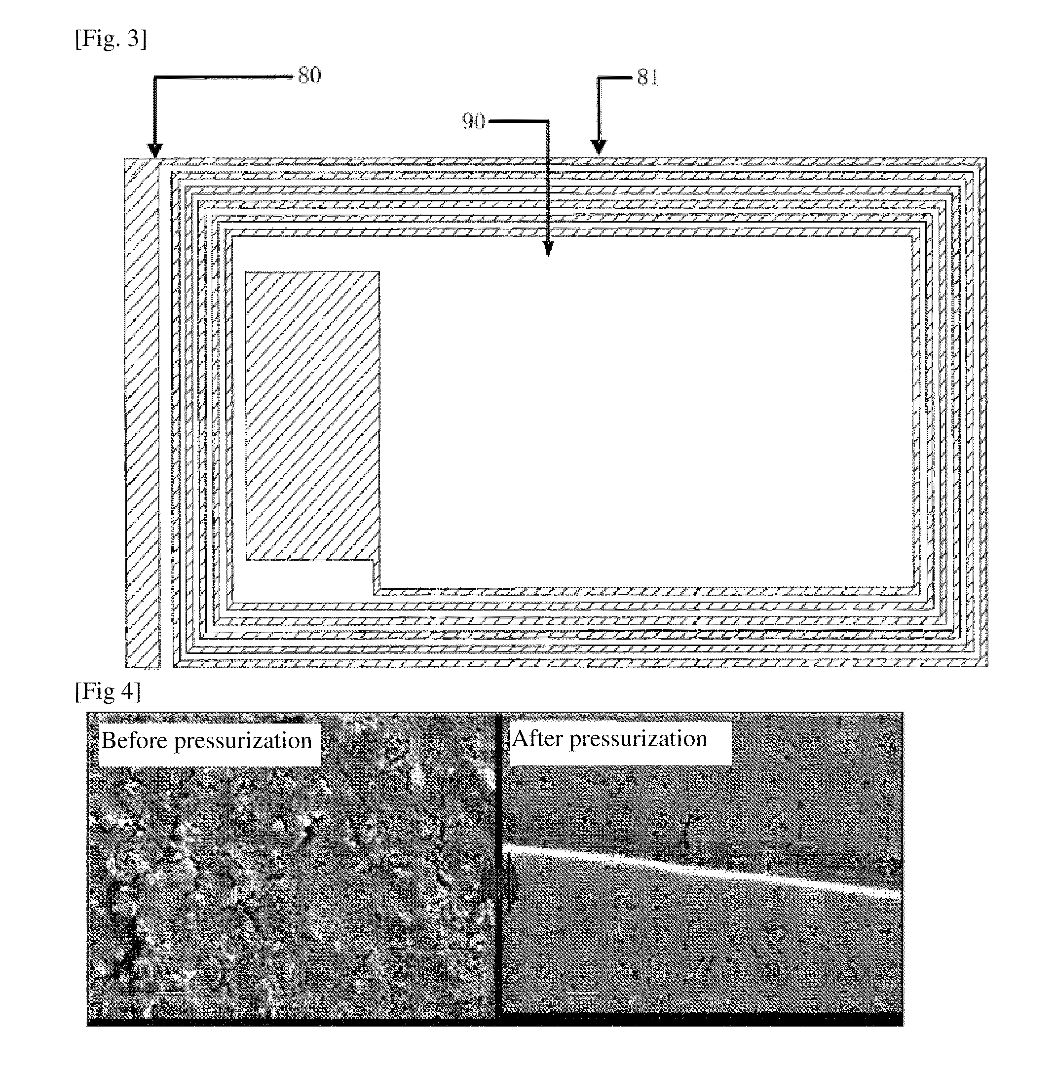
[0144]A printed silver wiring with a wire width of 1 mm, film thickness of approx. 12 μm and overall length of 100 mm was formed on a PET substrate using a screen printer and silver paste for screen printing. A micrometer (MDC-25MJ by Mitutoyo) was used in the measurement of film thickness. When this silver wiring was heated and pressurized using a roller press equipped with an infrared heating mechanism, the film thickness decreased to approx. 6 μm and metal gloss was observed on the surface. Although the roller temperature rose to 80° C. at this time as a result of heating by infrared light, the sample table remained at normal temperature. When the pressure distribution was measured at the time of pressurization using a pressure measurement sheet (Prescale (registered trademark) for medium pressure and high pressure by Fuji Photo Film), the measured pressures were within a range of 10 MPa to 100 MPa. Change in wiring dimension caused by heating and pressurization, other than chang...


PUM

PropertyMeasurementUnit
particle sizeaaaaaaaaaa
diameteraaaaaaaaaa
roughnessaaaaaaaaaa

Abstract

The present invention forms a conductive pattern using a simple process on a general plastic substrate having flexibility, and also provides a conductive pattern forming film that allows for easy formation of a conductive pattern using an apparatus that performs a simple process of oriented pressurization at low temperature, as well as a method for forming conductive pattern and a conductive pattern forming apparatus for the same.
The conductive pattern forming film provides a pattern formed on a film substrate having flexibility by pressurizing, under heating, a conductive paste in which powder or fine particles of metal or semiconductor are dispersed and filled. The conductive pattern forming apparatus comprises a sample installation table having a flat placement surface, and a driving body for pressure application which is placed in a manner facing the placement surface and movable, wherein the driving body for pressure application is equipped with a support which is constituted by a flat metal panel having metal spheres along its bottom face.

Description

TECHNICAL FIELD [0001]The present invention relates to a conductive pattern forming film that allows for manufacturing of flexible electronic devices at low cost, as well as a method for forming conductive pattern and a conductive pattern forming apparatus for the same, and particularly to a method and apparatus for forming a conductive pattern on a film substrate having flexibility at low temperature and with ease.PRIOR ART [0002]In recent years, there have been expectations that flexible sheet displays, flexible RF-ID (radio frequency identification) systems and other user-friendly electronic devices will become rapidly popular. To make this a reality, electronic device patterns must be formed on flexible plastic films. Application of a printing process is being considered as a means for forming these electronic device patterns in large volumes at low cost.[0003]Traditionally, the mainstream method for forming fine wiring patterns has been to apply patterning under the photo-litho...

Claims


Application Information

Patent Timeline
Patent Type & Authority Applications(United States)
IPC IPC(8): H05K1/09B28B3/00
CPCH05K1/0393H05K3/102H05K3/1283H05K2201/0257H05K2203/0278H05K2203/1105H01B1/22H01B13/0016H01B13/0026H05K1/09
Inventor KAMATA, TOSHIHIDEYOSHIDA, MANABU
Owner NAT INST OF ADVANCED IND SCI & TECH
Why Eureka
Try Eureka