Method for cleaning optical element of EUV light source device and optical element cleaning device

a technology of light source device and cleaning method, which is applied in the direction of photomechanical equipment, instruments, and cleaning using liquids, etc., can solve the problems of difficult to overcome the influence of neutral particles and/or ions emitted from the plasma and target, difficult to maintain, and extremely expensive, etc., to achieve the effect of prolonging the usable life of the optical element and being easy to overcom

Active Publication Date: 2010-02-04
GIGAPHOTON
View PDF7 Cites 49 Cited by
  • Summary
  • Abstract
  • Description
  • Claims
  • Application Information

AI Technical Summary

Benefits of technology

[0018]A first aspect of the present invention provides a method for cleaning an optical element of an extreme ultraviolet light source device for removing, from the optical element in a chamber, scattered matter generated together with extreme ultraviolet light by plasma formed through laser beam excitation of a target in the chamber, the method comprising: making the scattered matter generated by the plasma no larger than nanosize by using solid tin as the target and using a CO2 laser as an excitation source of the solid tin; and imparting, to the scattered matter no larger than the nanosize adhered to the optical element, an effect of overcoming the adherence of the scattered matter.
[0019]A second aspect of the present invention provides an optical element cleaning device for an extreme ultraviolet light source device for removing, from the optical element in a chamber, scattered matter generated together with extreme ultraviolet light by plasma formed through laser beam excitation of a target in the chamber, wherein solid tin is used as the target, a CO2 laser is used as an excitation source of the solid tin, and the optical element cleaning device comprises cleaning means for imparting, to nanosize scattered matter adhered to the optical element generated by plasma formed through excitation of the solid tin by the CO2 laser, an effect of overcoming the adherence of the scattered matter.
[0029]A twelfth aspect of the present invention provides the optical element cleaning device for an extreme ultraviolet light source device as claimed in the second aspect of the present invention, wherein the optical element comprises a transmissive protective plate, provided between a plasma generation region and another optical element in such a way so as to cover the other optical element, for preventing scattered matter from adhering to the other optical element.
[0030]In the EUV light source device of the present invention, solid tin is used as a target, and a CO2 laser is used as a target excitation source, such that the debris generated by plasma formed through excitation of the solid tin (Sn) by a laser beam outputted by the CO2 laser has a size no greater than nanosize, as a result of which the nanosize debris adhered to the optical element is imparted the effect of overcoming debris adherence.
[0033]In the present invention, the debris generated by the plasma resulting from exciting a solid tin target with a CO2 laser is nanosize debris. The adherence of nanosize debris is very weak and is thus easy to overcome. Therefore, the nanosize debris can be removed from the optical element by subjecting the nanosize debris adhered to the optical element to the action of such forces or energy that can overcome that adherence. The usable life of the optical element can thus be prolonged as a result.

Problems solved by technology

In such an LPP-type EUV light source device, the influence of neutral particles and / or ions emitted from the plasma and target becomes problematic, in particular, when using a solid target.
In order to maintain a high reflectance in the EUV collector mirror, the latter must exhibit high surface flatness, for instance of about 0.2 nm (rms), which is extremely expensive.
As a result, frequent replacement of the EUV collector mirror incurs not only longer maintenance downtime but also increased operative costs.
In particular, the output of the EUV light source device increases when debris adheres to the optical elements provided in the optical path of laser beams and / or of the EUV light.
Adhesion of debris impairs also the sensitivity of any sensors or the like that may be provided on the optical elements.
However, the debris particles that form the metallic film have substantial adherence, and hence it has been impossible to fully remove debris from the optical elements, even when subjecting the debris adhered to the optical elements to physical cleaning.
Such a method, however, has the following problems when employed for cleaning an EUV collector mirror.
In addition to impairing as a result the flatness of the EUV collector mirror, this shortens also the life of the EUV collector mirror.
Herein, heating the optical element to a temperature of 300° C. or above gives rise to fatigue breakdown on account of differences in the coefficients of thermal expansion of the coating materials, and / or thermal diffusion among coating substances, all of which impair reflectance and / or transmissivity.
Conventional cleaning methods, therefore, have failed to prolong the usable life of EUV collector mirrors by preserving the original reflectance and transmissivity of the optical element over long periods of time.

Method used


Image

  • Method for cleaning optical element of EUV light source device and optical element cleaning device
  • Method for cleaning optical element of EUV light source device and optical element cleaning device
  • Method for cleaning optical element of EUV light source device and optical element cleaning device

Examples


example 1

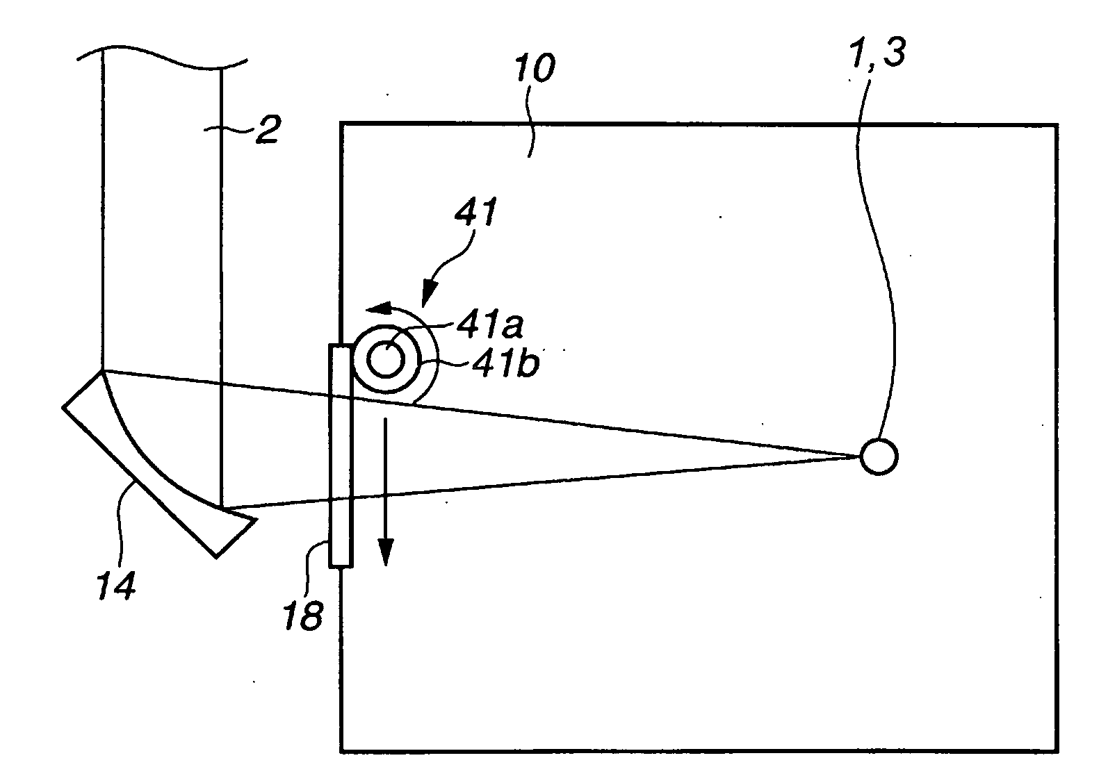
[0066]FIG. 5 is a diagram illustrating the constitution of a first embodiment. In FIG. 5, features identical to those of FIG. 1 are denoted with identical reference numerals, and the explanation thereof is omitted.

[0067]In the present embodiment, the adherence of the nanosize debris adhered to the input window 18 is overcome by wiping the output side surface of the input window 18.

[0068]A scrubber 41 is provided in the vicinity of the input window 18 inside the vacuum chamber 10. The scrubber 41 is a rotary brush comprising a brush 41b of a material such as nylon, mohair, PVA (polyvinyl alcohol), PP (polypropylene) or the like, provided around a cylindrical shaft 41a. A driving device not shown causes the scrubber 41 to slide over the input window 18 while rotating around the shaft axis. The scrubber 41 may be a fixed brush instead of a rotary brush.

[0069]The scrubber 41 may be imparted a weak chemical cleaning effect by wetting the brush 41b with a cleaning solution, for instance, ...

example 2

[0073]FIG. 6 is a diagram illustrating the constitution of a second embodiment. In FIG. 6, features identical to those of FIG. 1 are denoted with identical reference numerals, and the explanation thereof is omitted.

[0074]In the present embodiment, the adherence of nanosize debris to a debris protective plate 46 (having as a material thereof any among ZnSe, BaF2, NaCl, Si, Ge, CsI and KRS-5) provided on the output side of the input window 18 is overcome through wiping of the surface of the debris protective plate 46.

[0075]A cleaning chamber 45 is partitioned off in the interior of the vacuum chamber 10, in the vicinity of the input window 18, in such a way so as not to hinder the laser beam 2. The debris protective plate 46, shaped as a circular plate, is pivotably supported inside the cleaning chamber 45. The debris protective plate 46 is a transmissive optical element formed of, for instance, zinc selenium (ZnSe), barium fluoride or the like (BaF2) or the like. Part of the debris p...

example 3

[0080]FIG. 7 is a diagram illustrating the constitution of a third embodiment. In FIG. 7, features identical to those of FIG. 1 are denoted with identical reference numerals, and the explanation thereof is omitted.

[0081]In the present embodiment, the adherence of nanosize debris adhered to the reflective surface of the EUV collector mirror 15 is overcome by sputtering (plasma etching) in which plasma is biased.

[0082]Inside the vacuum chamber 10 there are provided a planar electrode 51, comprising a conductive substrate, connected to the rear face of the EUV collector mirror 15, and a grid electrode 52 facing the reflective surface of the EUV collector mirror 15, so as to flank the generation region of the plasma 3. The planar electrode 51 is connected to a 13.56 MHz RF power supply 54 via a blocking capacitor 53. The grid electrode 52 is connected to ground. In such a configuration, the planar electrode 51 is the cathode and the grid electrode 52 is the anode.

[0083]A gas supply devi...


PUM

PropertyMeasurementUnit
wavelengthaaaaaaaaaa

Abstract

A method for cleaning an optical element of an extreme ultraviolet light source device for removing, from the optical element in a chamber, scattered matter generated together with extreme ultraviolet light by plasma formed through laser beam excitation of a target in the chamber, the method which comprises: making the scattered matter generated by the plasma no larger than nanosize by using solid tin as the target and using a CO2 laser as an excitation source of the solid tin; and imparting, to the scattered matter no larger than the nanosize adhered to the optical element, an effect of overcoming the adherence of the scattered matter.

Description

BACKGROUND[0001]1. Technical Field[0002]The present invention relates to an optical element cleaning method, and an optical element cleaning device, for cleaning an optical element having adhered thereon scattered material, generated together with EUV (extreme ultraviolet) light, in an EUV light source device employed as a light source in exposure apparatuses.[0003]2. Related Art[0004]In the wake of ever finer semiconductor processing in recent years, features are quickly becoming finer as well in photolithography. Fine processing requirements are moving from the 100 nm to the 70 nm node, and beyond, to the 50 nm node, in next-generation applications. To meet the requirements of fine processing at the 50 nm node or less, for instance, exposure apparatuses being developed are expected to combine an EUV light source having a wavelength of about 13 nm with a reducing projection reflective optical system (catadioptric system).[0005]There are three types of EUV light sources: LPP (laser ...

Claims


Application Information

Patent Timeline
Patent Type & Authority Applications(United States)
IPC IPC(8): C23C14/34B08B7/00
CPCH05G2/001G03F7/70033H05G2/005
Inventor MORIYA, MASATOUENO, YOSHIFUMIABE, TAMOTSUSUMITANI, AKIRA
Owner GIGAPHOTON
Why Eureka
Try Eureka