

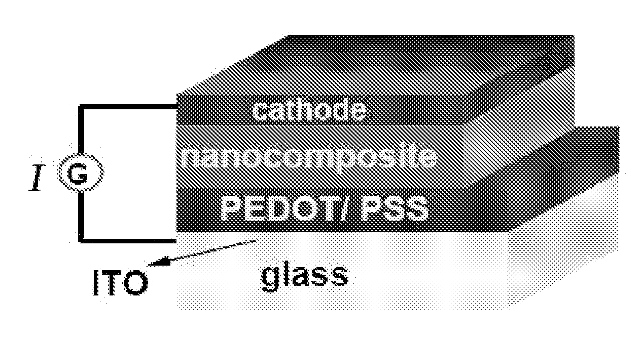
High density coupling of quantum dots to carbon nanotube surface for efficient photodetection
a quantum dot and carbon nanotube technology, applied in sustainable manufacturing/processing, camera filters, instruments, etc., can solve the problems of inefficient transfer of charge carriers to and from photosensitive qds, relative inefficiency of qd devices, and short efficiencies of hybrid polymer-qd devices, etc., to achieve high external quantum efficiency (eqe), efficient extraction of electron holes, and high density attachment of semiconductor qds
- Summary
- Abstract
- Description
- Claims
- Application Information
AI Technical Summary
Benefits of technology
Problems solved by technology
Method used
Image

Examples
example 1
Efficient Photodetection at Infrared Wavelengths by Incorporation of PbSe / Carbon Nanotube Conjugate in a Polymeric Nanocomposite
[0037]The thrust of the experimental study described in Examples 1-3 was to investigate the photodetection efficiency of a polymeric nanocomposite well sequestered with the IR active PbSe QDs and conducting SWNT, both being chemically attached to each other by a novel procedure. PbSe QDs, endowed with a high Bohr radius, exhibits excellent quantum size effects, and can be tuned to a precisely targeted wavelength of absorption in the IR region. Therefore, a stable SWNT-PbSe conjugate by chemical bonding of both components can be a promising candidate for efficient optoelectronic behavior in the IR. The large interfaces in the SWNT-PbSe composite proffer a tremendous opportunity for efficient exciton dissociation after photogeneration in the PbSe QDs. Efficient dissociation and charge transfer depend on the difference in the potential energy and electron affi...
example 2
Experimentals: Efficient Photodetection at Infrared Wavelengths by Incorporation of PbSe / Carbon Nanotube Conjugate in a Polymeric Nanocomposite
[0046]PbSe QDs were prepared as per our earlier report (Choudhury et al., Appl. Phys. Lett. 87:073110 (2005), which is hereby incorporated by reference in its entirety). Briefly, PbO (5 mmol) and oleic acid (25 mmol) were added to 20 mL tri-n-octyylamine. The reaction mixture was heated under alternate vacuum and argon atmosphere for 30 minutes at 155° C., when 10 mL IM selenium dissolved in tri-n-octylphosphine (TOP-Se) was rapidly injected into the reaction flask. A monodispersed crop of PbSe QDs were formed by this reaction, which could be retrieved at different size fractions. The QDs were cleaned off excess surfactant, oleic acid, and other side products by adding excess acetone to an aliquot and centrifugation.
[0047]The procedure of attaching PbSe QDs onto SWNT is given below: First, the SWNT (diam. 1.2-1.5 nm, length ...
example 3
Sample Characterization: Efficient Photodetection at Infrared Wavelengths by Incorporation of PbSe / Carbon Nanotube Conjugate in a Polymeric Nanocomposite
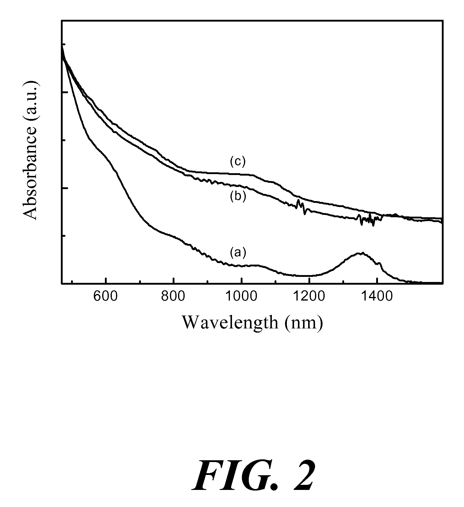
[0049]Absorption spectra were recorded using a Shimadzu 3101PC spectrophotometer. A SPEX 270M spectrometer (Jobin Yvon) equipped with an InGaAs photodetector (Electro-Optical Systems Inc., USA) was used for acquisition of PL emission spectra. An argon ion laser (BeamLok, Spectra-Physics) (488 nm line) was used for PL excitation. Excitation power was maintained the same for every round of acquisition. The samples in quartz cuvettes were mounted directly in front of the entrance slit of the spectrometer and the exciting laser beam was directed at 90-degrees relative to the collection of emission.
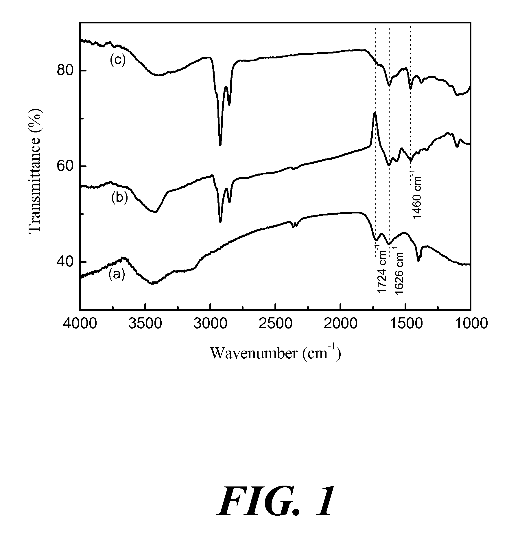
[0050]FT-IR spectra of carboxylated SWNT, thiolated SWNT and SWNT-PbSe conjugates in KBr pellets were obtained. These measurements were made using a Perkin Elmer FT-IR spectrometer model 1760X operating in transmission mode. Transmission Elect...
PUM
| Property | Measurement | Unit |
|---|---|---|
| External quantum efficiency | aaaaa | aaaaa |
| Density | aaaaa | aaaaa |
| Electric charge | aaaaa | aaaaa |
Abstract
Description
Claims
Application Information