Amorphous carbon film, semiconductor device, film forming method, film forming apparatus and storage medium

a technology of amorphous carbon film and semiconductor devices, which is applied in the direction of coatings, basic electric elements, chemical vapor deposition coatings, etc., can solve the problems of deterioration of cu wiring conductivity, disadvantages of amorphous carbon, and low elastic modulus of the material

Inactive Publication Date: 2010-02-11
TOKYO ELECTRON LTD
View PDF4 Cites 25 Cited by
  • Summary
  • Abstract
  • Description
  • Claims
  • Application Information

AI Technical Summary

Benefits of technology

[0010]In accordance with the present invention, the amorphous carbon film may be used as a barrier film for preventing an element of a wiring metal in one wiring circuit from being diffused into an interlayer insulating film of an adjacent wiring circuit.

Problems solved by technology

However, the amorphous carbon is disadvantageous in that an elastic modulus thereof is low.
For example, in case of using the amorphous carbon film as the barrier film as described above, if a reduction ratio of the film thickness, a so-called film thickness reduction, is high, the amorphous carbon film is peeled off from the wiring and the interlayer insulating film, resulting in a deterioration of Cu wiring conductivity.

Method used


Image

  • Amorphous carbon film, semiconductor device, film forming method, film forming apparatus and storage medium
  • Amorphous carbon film, semiconductor device, film forming method, film forming apparatus and storage medium
  • Amorphous carbon film, semiconductor device, film forming method, film forming apparatus and storage medium

Examples


application example 1

Other Application Example 1

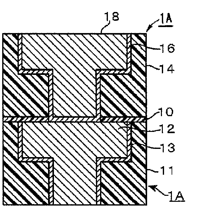
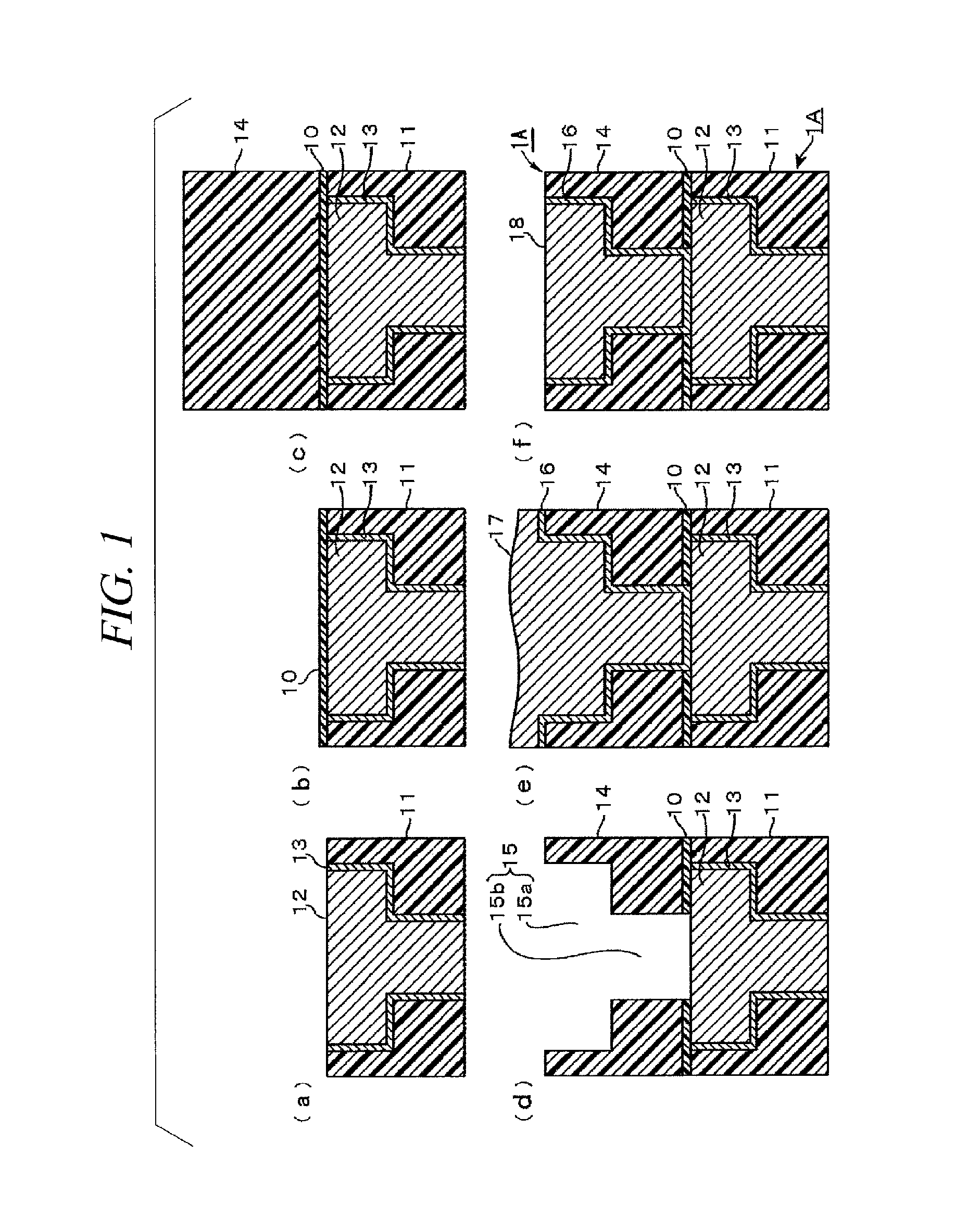
[0062]In this example, an amorphous carbon film of the present invention is used as a hard mask for forming a recess portion for burying a copper wiring 12 in an interlayer insulating film 80 made up of a CF film. The hard mask functions as a mask in an etching process and does not affect a property of a device even if it remains thereon. In this example, the hard mask is used for maintaining a function as a mask after a resist mask disappears in the etching process. As an example of this embodiment, a case where a (n+1)th wiring circuit is formed on an nth (n is integer of 1 or greater) wiring circuit will be explained with reference to FIG. 5. Furthermore, in FIG. 5, a film which is the same as the wiring circuit of FIG. 1 is assigned the same reference numeral, and the CF film 80, instead of the SiCOH films 11 and 14, is used for the purpose of a high-speed operation of the semiconductor device but a low dielectric constant film having an upper and lowe...

application example 2

Other Application Example 2

[0069]In addition, the amorphous carbon film of the present invention can be used as an anti-reflection film for preventing a light irradiated on a substrate surface from scattering during exposure process. In this regard, there will be an explanation with reference to FIGS. 7 and 8. First of all, in the present example, as illustrated in FIG. 7, a SiOCH film 200 having a low dielectric constant and the amorphous carbon film 10 of the present invention are formed on the substrate surface in sequence (FIG. 7(a)), and the process-completed wafer is accommodated in the carrier 90. Then, the carrier 90 is transferred to a coating and developing apparatus 202 by a transfer robot 201. In the coating and developing apparatus 202, formed on the amorphous carbon film 10 is a chemically amplified resist film 203, for example (FIG. 7(b)). Subsequently, an exposure process is performed on the resist film 203 (FIG. 7(c)). At this time, if the resist film 203 is a negat...

application example 3

Other Application Example 3

[0072]Besides, the amorphous carbon film of the present invention can be used as an insulating layer embedding a transistor therein instead of a BPSG (Boron Phosphorous Silicate Glass) film. In this manner, by using the amorphous carbon film as the insulating layer embedding the transistor, it is possible to reduce a parasitic capacitance incurred between a wiring and a gate electrode in the transistor. FIG. 9 illustrates a CMOS transistor employing the amorphous carbon of the present invention as the insulating layer. In FIG. 9, a reference numeral 210 denotes a p-type silicon layer, a reference numeral 220 denotes a n-well layer, a reference numeral 230 denotes a p-well layer, reference numerals 221 and 222 denote p+-type portions serving as a source and a drain respectively, reference numerals 231 and 232 denote n+-type portions serving as a source and a drain respectively, a reference numeral 211 denotes a gate oxide film, a reference numeral 212 denot...


PUM

PropertyMeasurementUnit
dielectric constantaaaaaaaaaa
internal pressureaaaaaaaaaa
temperatureaaaaaaaaaa

Abstract

Provided is an amorphous carbon film having a high elastic modulus and a low thermal contraction rate with a suppressed low dielectric constant, a semiconductor device including the amorphous carbon film and a technology for forming the amorphous carbon film. Since the amorphous carbon film is formed by controlling an additive amount of Si (silicon) during film formation, it is possible to form the amorphous carbon film having a high elastic modulus and a low thermal contraction rate with a suppressed dielectric constant as low as 3.3 or less. Accordingly, when the amorphous carbon film is used as a film in the semiconductor device, troubles such as a film peeling can be suppressed.

Description

TECHNICAL FIELD[0001]The present invention relates to an amorphous carbon film used in, e.g., a semiconductor device and a technology of forming the amorphous carbon film.BACKGROUND ART[0002]In a process for manufacturing a semiconductor device, there is performed a damascene process in which a recess portion is formed in an interlayer insulating film made of a low dielectric constant, called as low-k, material such as a CF film (fluorine-containing carbon film) or a SiCOH film (film containing silicon, oxygen, carbon, and hydrogen) and then a wiring made of Cu (copper) is formed in such a recess portion. In the damascene process, formed between the Cu wiring and the interlayer insulating film is a barrier film for suppressing a diffusion of the Cu into the interlayer insulating film. The barrier film has been made of, e.g., SiCN (silicon carbon nitride) made up mainly of silicon and having Si atomic ratio of 50% or more therein, for example. However, in order to achieve a high-spee...

Claims


Application Information

Patent Timeline
Patent Type & Authority Applications(United States)
IPC IPC(8): H01L23/532H01L21/314C09D1/00
CPCC23C16/26H01L21/0276H01L21/31144H01L21/3146H01L23/53295H01L21/76834H01L21/76835H01L23/53238H01L23/5329H01L21/76811H01L2924/0002H01L21/02123H01L21/02274H01L21/02115H01L2924/00H01L21/31H01L21/768H01L23/522
Inventor KIKUCHI, YOSHIYUKIKOBAYASHI, YASUOKAWAMURA, KOHEINOZAWA, TOSHIHISAISHIKAWA, HIRAKU
Owner TOKYO ELECTRON LTD
Why Eureka
Try Eureka