Silicon wafer, method for manufacturing the same and method for heat-treating the same

a technology of silicon wafers and heat-treating methods, which is applied in the direction of polycrystalline material growth, crystal growth process, after-treatment details, etc., can solve the problems of reducing the yield of the device, difficult to prevent the generation of vacancy-type point defects, and increasing the quality requirements of the silicon wafer to be used as a substrate of such semiconductor devices, so as to improve the reduction capacity of grown-in defects and suppress the generation of slips

Active Publication Date: 2010-02-18
GLOBALWAFERS JAPAN
View PDF15 Cites 29 Cited by
  • Summary
  • Abstract
  • Description
  • Claims
  • Application Information

AI Technical Summary

Benefits of technology

[0045]A first illustrative aspect of the present invention provides a method of manufacturing a silicon wafer capable of imp...

Problems solved by technology

With trends toward high integration of semiconductor devices in recent years, requirement for the quality of a silicon wafer to be used as a substrate of such semiconductor devices is becoming severer.
Of these grown-in defects, generation of agglomerates (dislocation clusters) of interstitial silicon-type point defects can be prevented by adjusting pull-up conditions upon pulling up single crystals, but it is very difficult to prevent generation of the agglomerates of vacancy-type point defects or the oxide precipitates.
When the oxide precipitates exist in the device active region, on the other hand, they are not preferred because they may be a cause for reducing a device yield.
However, in the wafer subjected to RTP in an oxidizing atmosphere at a high temperature of 1,300° C. or more, the range of DZ layer is wide and it is difficult to sufficiently getter impurities or suppress generation of a slip ascribable to a thermal stress.
However, in the heat treatment method described in Patent Document 11, since a heat treatment is performed for a long time, the productivity decreases and the production cost at the heat treatment increases.
Also, the surface part of a wafer subjected to a long-time heat treatment undergoes reduction of the concentration of solid-solution oxygen in the silicon resulting from out-diffusion of oxygen and when such a wafer is used in the device process, the dislocation generated by the application of stress or distortion produced in the device process is liable to extend, giving rise to reduction of the devi...

Method used


Image

  • Silicon wafer, method for manufacturing the same and method for heat-treating the same
  • Silicon wafer, method for manufacturing the same and method for heat-treating the same
  • Silicon wafer, method for manufacturing the same and method for heat-treating the same

Examples


example 1

[0166]Advantages of the first embodiment of the invention will hereinafter be described using Examples 1-1 to 1-4, but the invention is not limited to or by Examples 1-1 to 1-4.

example 1-1

[0167]A silicon single crystal ingot having a P type, a crystal plane direction (001), a concentration [Oi] of oxygen solid solution of 1.2×10¹⁸ atoms / cm3 (calculated from a conversion factor based on Old ASTM), and a resistance of from 23 to 25 Ω / cm was produced by the CZ process.

[0168]Nitrogen doping treatment was performed by filling the crucible with a silicon wafer coated with a silicon nitride film and a pull rate V was adjusted to 1.2 mm / min on average and at the same time, the pull rate V and a temperature gradient G at 1300° C. in the direction of a crystal axis were controlled to control a V / G ratio in order to prevent generation of dislocation clusters during the growth of a silicon single crystal.

[0169]The resulting silicon single crystal ingot was then sliced into a wafer by a wire saw and subjected to beveling, lapping, etching, and polishing to obtain a double-side polished silicon wafer having a diameter of 300 mm.

[0170]Then, from the same lot of the silicon wafers t...

example 1-2

[0176]A double-side polished silicon wafer having a diameter of 300 mm was prepared in a similar manner to Example 1-1 except for the use of a silicon single crystal ingot prepared by the CZ process and having a P type, a crystal plane direction (001), a concentration [Oi] of oxygen solid solution of 1.0×10¹⁸ atoms / cm3 (calculated from a conversion factor based on Old ASTM), and a resistance of from 28 to 30 Ω / cm.

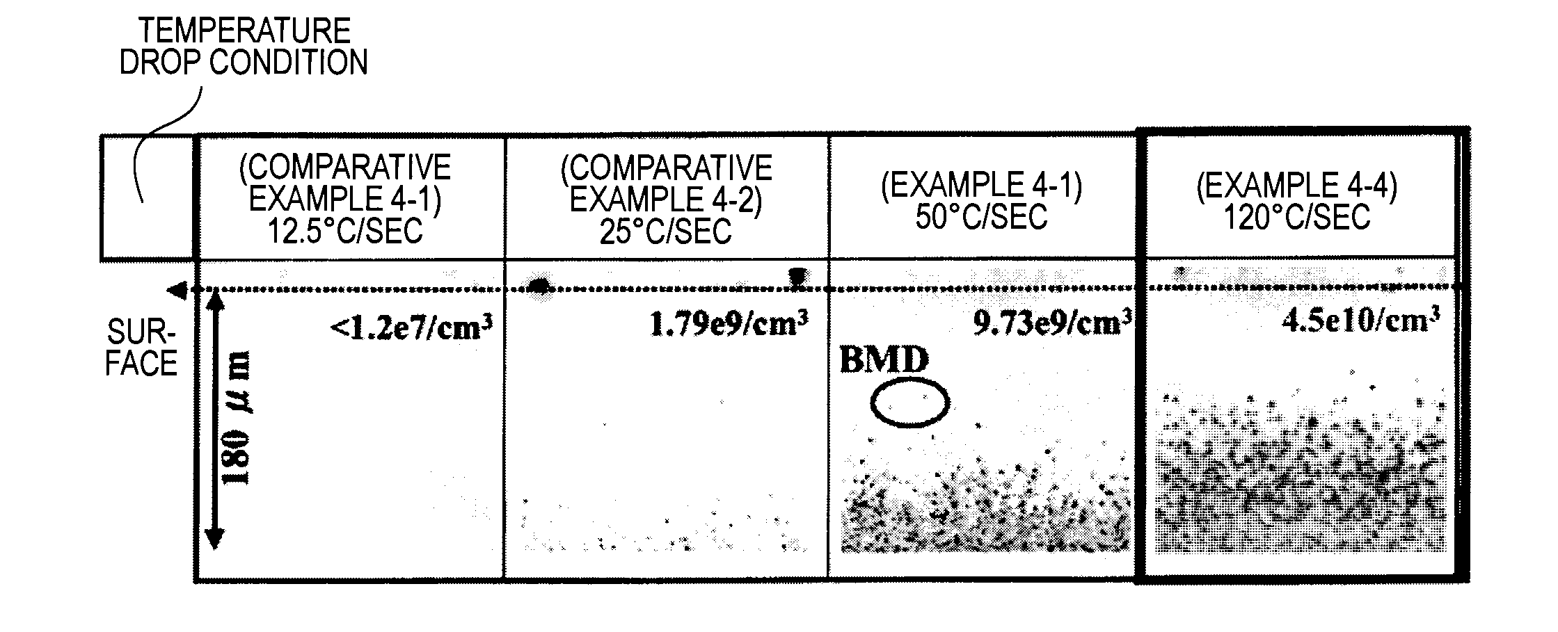
[0177]Then, several silicon wafers were sampled from the same lot and grown-in defects in the device surface of the silicon wafers thus sampled were observed with AFM. The maximum size of the thus-observed grown-in defects in terms of a diameter of a sphere having a volume equal to that of the grown-in defects was measured. As a result, the maximum size of COP measured in Example 1-2 was 100 nm.

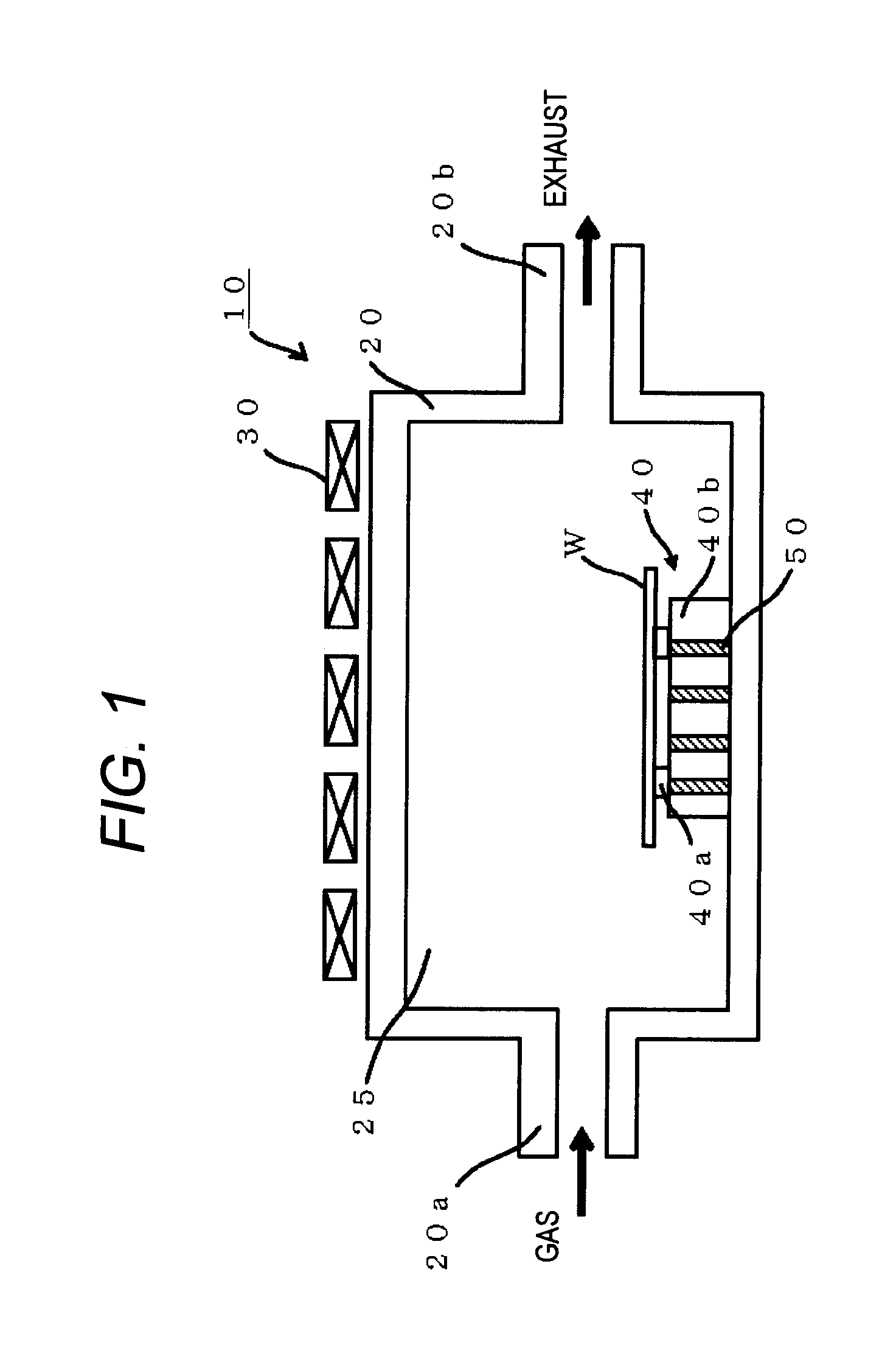
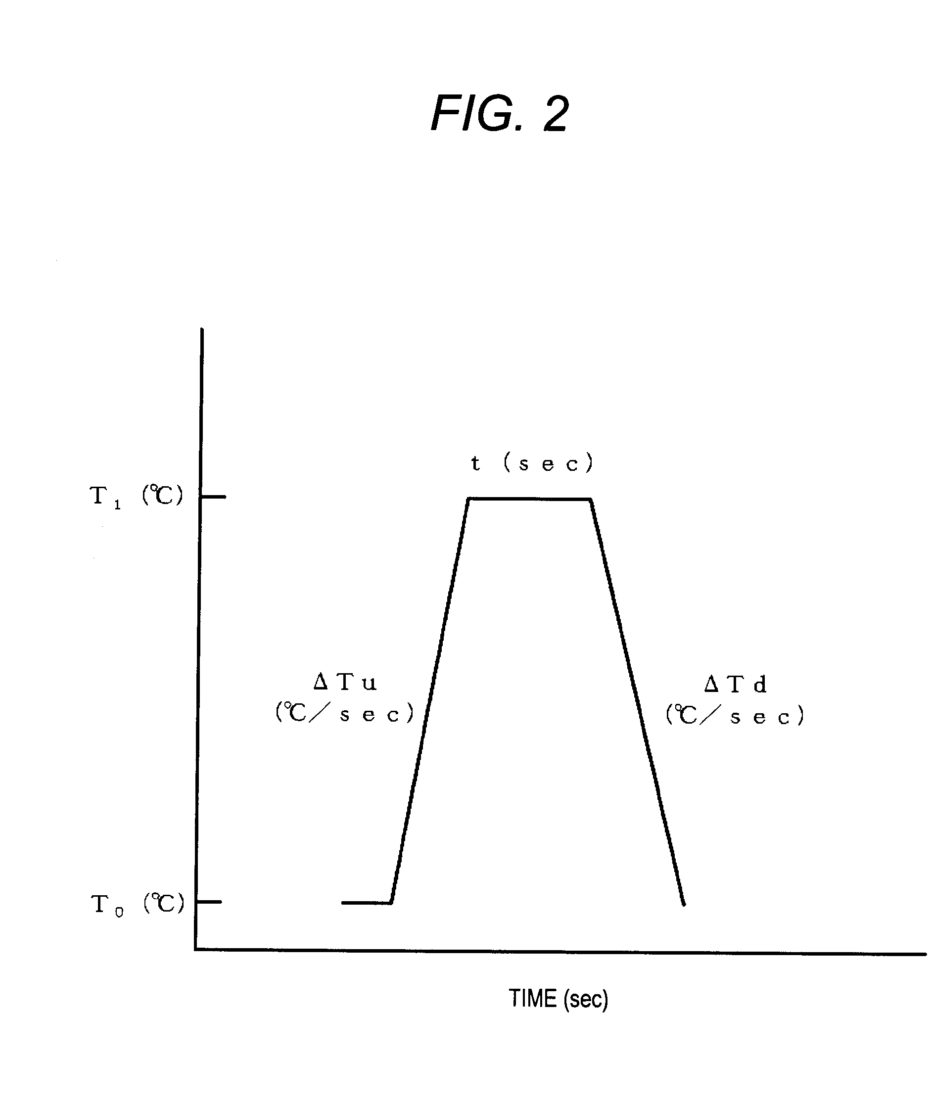
[0178]Then, using an RTP apparatus 10 as illustrated in FIG. 1, a rapid heating / cooling thermal process of the silicon wafers was performed. In Example 1-2, the rapid heating / cooling...


PUM


Abstract

A silicon wafer produced from a silicon single crystal ingot grown by Czochralski process is subjected to rapid heating/cooling thermal process at a maximum temperature (T1) of 1300° C. or more, but less than 1380° C. in an oxidizing gas atmosphere having an oxygen partial pressure of 20% or more, but less than 100%. The silicon wafer according to the invention has, in a defect-free region (DZ layer) including at least a device active region of the silicon wafer, a high oxygen concentration region having a concentration of oxygen solid solution of 0.7×10¹⁸ atoms/cm3 or more and at the same time, the defect-free region contains interstitial silicon in supersaturated state.

Description

[0001]This application claims priority from Japanese Patent Application No. 2008-198680, filed on Jul. 31, 2008, Japanese Patent Application No. 2008-198681, filed on Jul. 31, 2008, Japanese Patent Application No. 2009-044379, filed on Feb. 26, 2009, and Japanese Patent Application No. 2009-054703, filed on Mar. 9, 2009, the entire contents of which are hereby incorporated by reference.FIELD OF THE INVENTION[0002]The present disclosure relates to a silicon wafer and a method for manufacturing the silicon wafer to be used as a substrate of semiconductor devices.[0003]In addition, the present disclosure relates to a method for heat-treating the silicon wafer. The method is performed in order to apply the silicon wafer obtained by slicing a silicon single crystal ingot by a Czochralski process to semiconductor device.DESCRIPTION OF RELATED ART[0004]With trends toward high integration of semiconductor devices in recent years, requirement for the quality of a silicon wafer to be used as ...

Claims


Application Information

Patent Timeline
IPC IPC(8): H01L29/36H01L21/26H01L21/322
CPCC30B29/06H01L21/324H01L21/3225C30B33/02C30B15/22
Inventor ISOGAI, HIROMICHISENDA, TAKESHITOYODA, EIJIMURAYAMA, KUMIKOIZUNOME, KOJIMAEDA, SUSUMUKASHIMA, KAZUHIKOARAKI, KOJIAOKI, TATSUHIKOSUDO, HARUOMOCHIZUKI, YOICHIROKOBAYASHI, AKIHIKOFU, SENLIN
Owner GLOBALWAFERS JAPAN
Why Eureka
Try Eureka