Raman spectroscopy

a raman spectroscopy and spectroscopy technology, applied in radiation pyrometry, instruments, material analysis, etc., can solve the problems of raman spectroscopy drawbacks, high power sources that are not only bulky and expensive, and place an upper limit on the intensity of optical radiation sources, so as to improve the performance of the sour

Inactive Publication Date: 2010-03-18
UNIV OF SOUTHAMPTON
View PDF14 Cites 21 Cited by
  • Summary
  • Abstract
  • Description
  • Claims
  • Application Information

AI Technical Summary

Benefits of technology

[0009]According to a first aspect of the invention, there is provided a spectrometer for obtaining a Raman spectrum from a sample material. The spectrometer comprises an optical source for generating optical radiation, a substrate for receiving the optical radiation, and a spectral analyser for analysing the Raman scattered radiation emerging from the substrate. The substrate comprises a metallic film that incorporates a plurality of voids of a predetermined size. These voids are suitable for confining surface plasmons. The surface plasmons couple energy from incident optical radiation to a sample material when the sample material is located proximal the substrate. The surface plasmons are also responsible for converting scattered energy emitted from the sample material into the Raman scattered radiation. The substrate may be incorporated into existing Raman spectrometers in order to improve their performance.
[0010]The substrate provides an enhanced Raman signal. Therefore to obtain an acceptable SNR, less incident optical radiation or a lower sensitivity detector can be used, or both. In various embodiments, the spectral analyser makes use of detectors that do not need to be cooled, such as a photodiode array. Certain embodiments can make use of high efficiency compact optical source devices, such as a laser diode or laser diode array. By employing such detectors and arrays, a high efficiency, low-power, portable, and compact Raman spectrometer can be provided. Moreover, embodiments employing, for example, a laser diode array provide optical radiation that can be used to illuminate large area of substrate. In various such embodiments, it is not always necessary to focus the optical radiation, thereby further improving the compactness and reducing the cost of these spectrometer.
[0011]Moreover, because of the enhanced Raman signal, input channel optics provided with the spectral analyser to collect Raman scattered radiation may be made to differ from optics used in conventional Raman spectrometers. In particular, various embodiments avoid the need to use a high numerical aperture lens system to collect Raman scattered radiation. This allows the collection optics to be spaced away from the substrate. Such spacing is particularly beneficial as it enables fluids containing sample material to be analysed to freely flow over the substrate without being impeded by the collection optics. The fluid may be liquid or gas. The input channel optics may comprise a fibre optic input channel oriented towards the substrate. As in various embodiments the direction of emerging Raman signal can be predicted, use of a fibre optic input channel can be used to cut down on any background signal from the optical source that reaches the spectral analyser.

Problems solved by technology

The principal drawbacks associated with Raman spectroscopy arise because of the small scattering cross-section.
This means that there are often problems related to separating out the small Raman signal from the large Rayleigh signal and the incident signal, especially when the Raman signal is close in energy to the incident signal.
High power sources are not only both bulky and expensive, but at very high power the intensity of the optical radiation itself can destroy the sample material, thus placing an upper limit on the optical radiation source intensity.
Similarly, high sensitivity detectors are often bulky and expensive, and even more so where forced cooling, such as with liquid nitrogen, is necessary.
Additionally, detection is often a slow process as long integration periods are required to obtain a Raman spectrum signal having an acceptable signal-to-noise ratio (SNR).
However, whilst SERS devices can lead to an improved SNR when compared to previous conventional Raman spectrometers, they still suffer to a lesser extent with various of the same disadvantages.
For example, SERS devices are still not efficient enough to provide a Raman signal without fairly long detector integration times, and can still require the use of bulky and expensive detectors.

Method used


Image

  • Raman spectroscopy
  • Raman spectroscopy
  • Raman spectroscopy

Examples


first embodiment

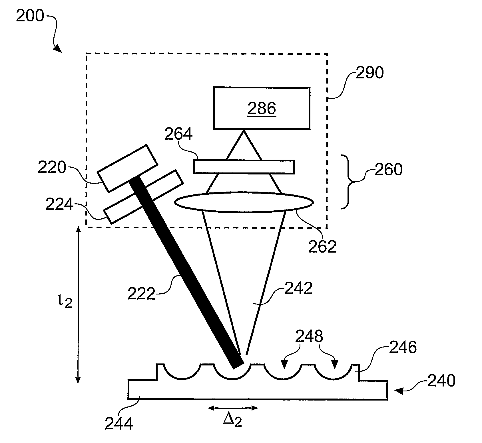
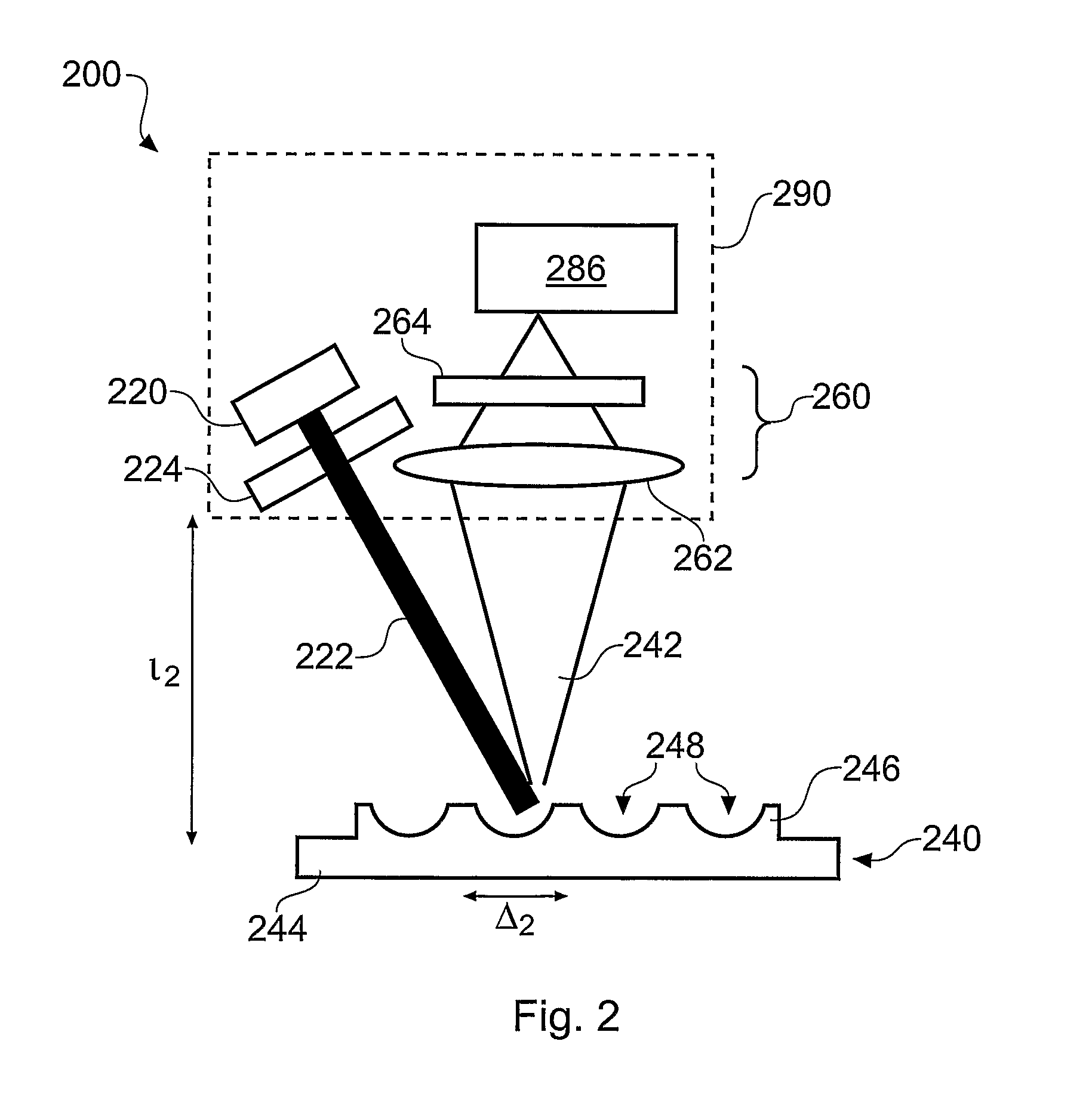
[0068]FIG. 2 shows a Raman spectrometer 200 according to the invention. The spectrometer 200 comprises a source / detector package 290 and a substrate 240. The source / detector package 290 comprises an optical source 220 and a first filter 224 for filtering optical radiation 222 generated by the optical source 220. The package 290 also includes input channel optics 260 and a spectral analyser 286.

[0069]The input channel optics 260 comprises a first lens 262 for gathering Raman scattered radiation 242 and a second filter 264 for rejecting any non-Raman scattered radiation. The input channel optics directs Raman scattered radiation to the spectral analyser 286.

[0070]The source / detector package 290 is configured to direct optical radiation 222 on to the surface of the substrate 240 and to collect Raman scattered radiation 242 that is generated by a sample that is placed proximal to the surface of the substrate 240. The substrate 240 comprises a support layer 244 with a metallic film 246 f...

second embodiment

[0074]FIG. 3 shows a Raman spectrometer 300 according to the invention. The spectrometer 300 comprises an optical source 320, a substrate 340 and a detector package 380.

[0075]The optical source 320 comprises a laser diode. The laser diode generates a beam of optical radiation 322 that is filtered by a first filter 324 to provide a monochromatic beam. The optical radiation 322 is coupled in to an optically transparent support layer 344 of the substrate 340. A blazed grating is written in to the support layer 344 for coupling the optical radiation 322 from the support layer 344 in to a metallic film 346 formed on the support layer 344. Optical radiation 322 excites plasmons in voids 348 that are formed in metallic film 346.

[0076]Sample material is placed in the voids 348 and excites Raman scattered radiation 342 in response to the plasmons generated by the optical radiation 322. The Raman scattered radiation 342 is emitted from the metallic film 346 in a direction that depends upon th...

third embodiment

[0079]FIG. 4 shows a Raman spectrometer 400 according to the invention. The Raman spectrometer 400 comprises an optical source 420 for generating optical radiation 422. The optical radiation 422 is filtered by a first filter 424 and guided in to an optically transparent support layer 444 formed in a substrate 440. The optical radiation 422 couples in to a metallic film 446 formed upon the support layer 444 over a distance of Δ4. The distance Δ4 can be greater than 100 micrometers.

[0080]Optical radiation 422 excites plasmons in voids 448 that are formed in the metallic film 446. The plasmons couple energy to sample materials that are located near the voids 448. The excited sample material gives rise to Raman scattered energy that couples via plasmons back in to the optically transparent support layer 444. The support layer 444 acts as a waveguide that guides Raman scattered radiation 442 through the support layer 444.

[0081]Detector package 480 is provided to detect the Raman scattere...


PUM

PropertyMeasurementUnit
diameteraaaaaaaaaa
sizeaaaaaaaaaa
diameteraaaaaaaaaa

Abstract

It has been discovered that specially structured metallic films containing voids can deliver a hugely enhanced surface enhanced Raman spectroscopy (SERS) effect. By selecting a particular size and geometry for the voids, metallic films can be provided which have an enhanced photon-to-plasmon conversion efficiency for incident radiation of a predetermined wavelength. Controllable surface-enhanced absorption and emission characteristics may thus be provided, which are useful for SERS and potentially also other optical spectrometry and filtering applications. With such a large Raman signal, the invention enables fast, compact and inexpensive Raman spectrometers to be provided opening up many new application possibilities.

Description

FIELD OF THE INVENTION[0001]The invention relates principally but not exclusively to Raman spectroscopy, in particular surface enhanced Raman spectroscopy (SERS).BACKGROUND OF THE INVENTION[0002]Raman spectroscopy is used for a variety of applications, most commonly to study vibrational quanta, such as vibrations in molecules or phonons in solids, although other quantised entities can also be studied. Raman spectroscopy can provide detailed information relating to the physical state of sample materials and can be used to distinguish various states of otherwise chemically identical molecules, such as various molecular isomers, from one another.[0003]Raman spectroscopy finds wide ranging use in numerous different industries. By way of example, Raman spectroscopy finds application in the pharmaceutical, chemical, bio-analysis, medical, materials science, art restoration, polymer, semiconductor, gemology, forensic, research, military, sensing and environmental monitoring fields.[0004]Al...

Claims


Application Information

Patent Timeline
Patent Type & Authority Applications(United States)
IPC IPC(8): G01J3/44G01N21/55G01N21/65
CPCG01N21/658
Inventor BAUMBERG, JEREMY J.ABDELSALAM, MAMDOUHBARTLETT, PHILLIP N.RUSSELL, ANDREASUGAWARA, YOSHIHIROPELFREY, SUZANNE
Owner UNIV OF SOUTHAMPTON
Why Eureka
Try Eureka