Thin film transistor and semiconductor device using the same

a thin film transistor and semiconductor technology, applied in the field of thin film transistors, can solve the problems of deterioration or unavoidable exposure of the side surfaces of the semiconductor, and fear of physical peeling of the semiconductor layer

Inactive Publication Date: 2010-04-15
HITACHI LTD
View PDF8 Cites 15 Cited by
  • Summary
  • Abstract
  • Description
  • Claims
  • Application Information

AI Technical Summary

Benefits of technology

[0005]When a thin film transistor is used as a switching driving element of a semiconductor device such as display or IC tag, it is necessary to form on the thin film transistor a passivation film having (1) dielectric property, (2) property as a barrier against oxygen, water and the like, (3) mechanical strengths such as abrasion resistance, and the like. A passivation film for an organic transistor can be formed by a dry process such as vacuum deposition method, but a wet process such as spin-coating method / printing method is simpler and cheaper and moreover has an advantage that various organic polymer materials can be used as a passivation film material. Furthermore, a film can be used as a passivation film by applying or heat-printing the film. However, when a passivation film is formed by a wet process such as spin-coating method / printing method, there is fear that a semiconductor film would be deteriorated or peeled physically by an organic solvent dissolving the passivation film material.
[0007]The objects of the present invention reside in preventing deterioration / peeling of a semiconductor film and in providing a high-performance organic thin film transistor and a semiconductor device using the same.
[0010]The first passivation film is formed in advance of the formation of the second passivation film and placed between the semiconductor layer and the second passivation film. Anywhere within the substrate there is no other material between said first passivation film and said second passivation film. The semiconductor layer is capped by the first passivation film so that not only the top surface but also the side surfaces are not exposed. Thereby, a solution used for washing the substrate and a solution for applying and forming the second passivation film can be prevented from penetrating into the semiconductor layer.
[0011]Furthermore, the first passivation film can be formed by dropping of liquid drops or contact printing / heat printing, and therefore peeling of the semiconductor layer can be reduced highly as compared with formation by spin-coating over the entire substrate. In addition, formation is carried out partly, and therefore the amount of material used can be reduced.
[0012]Moreover, by using as the first passivation film a material having a higher adhesion to a groundwork than the semiconductor layer and forming the first passivation film partly, contaminants which are attached to the portion not covered with the first passivation film and which lead to defects of a semiconductor device, can be removed by washing without peeling the semiconductor layer.
[0013]Furthermore, when a low molecular weight material such as pentacene is used as the semiconductor layer, it is desirable to use a water-soluble material as the first passivation film. The water-soluble material uses water as a solvent and hence hardly penetrates into the interface between pentacene and a groundwork and the semiconductor layer is not peeled from the groundwork. Moreover, deterioration of the channel portion is scarcely caused. Among water-soluble materials, particularly a light-sensitive material is suitable for the first passivation film, because after curing by ultraviolet ray irradiation it becomes water-insoluble and makes washing of the substrate possible. As a light-sensitive water-soluble material, there is, for example, a polyvinyl alcohol, in which an azido light-sensitive group, is acetal-bonded. A polyvinyl alcohol is inferior in property as a barrier against water and a solution, and therefore water contained in the polyvinyl alcohol is sufficiently removed by heating of the substrate or the like, and then the second passivation film protecting all of the members including the semiconductor layer is formed with silicon oxide, silicon nitride or the like superior in property as a barrier to the polyvinyl alcohol.

Problems solved by technology

However, when a passivation film is formed by a wet process such as spin-coating method / printing method, there is fear that a semiconductor film would be deteriorated or peeled physically by an organic solvent dissolving the passivation film material.
However, particularly when a substrate is washed in the state where a semiconductor layer is exposed, there is fear that the semiconductor layer would be peeled physically.
Moreover, even when a semiconductor is left as an island by use of a water-soluble resist such as PVA, it is unavoidable that side surfaces of the semiconductor would be exposed.

Method used


Image

  • Thin film transistor and semiconductor device using the same
  • Thin film transistor and semiconductor device using the same
  • Thin film transistor and semiconductor device using the same

Examples


example 1

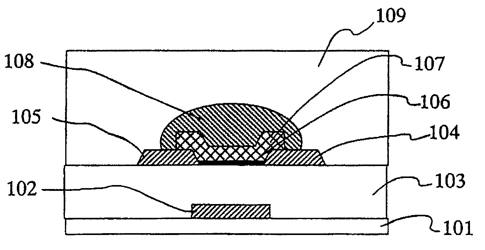
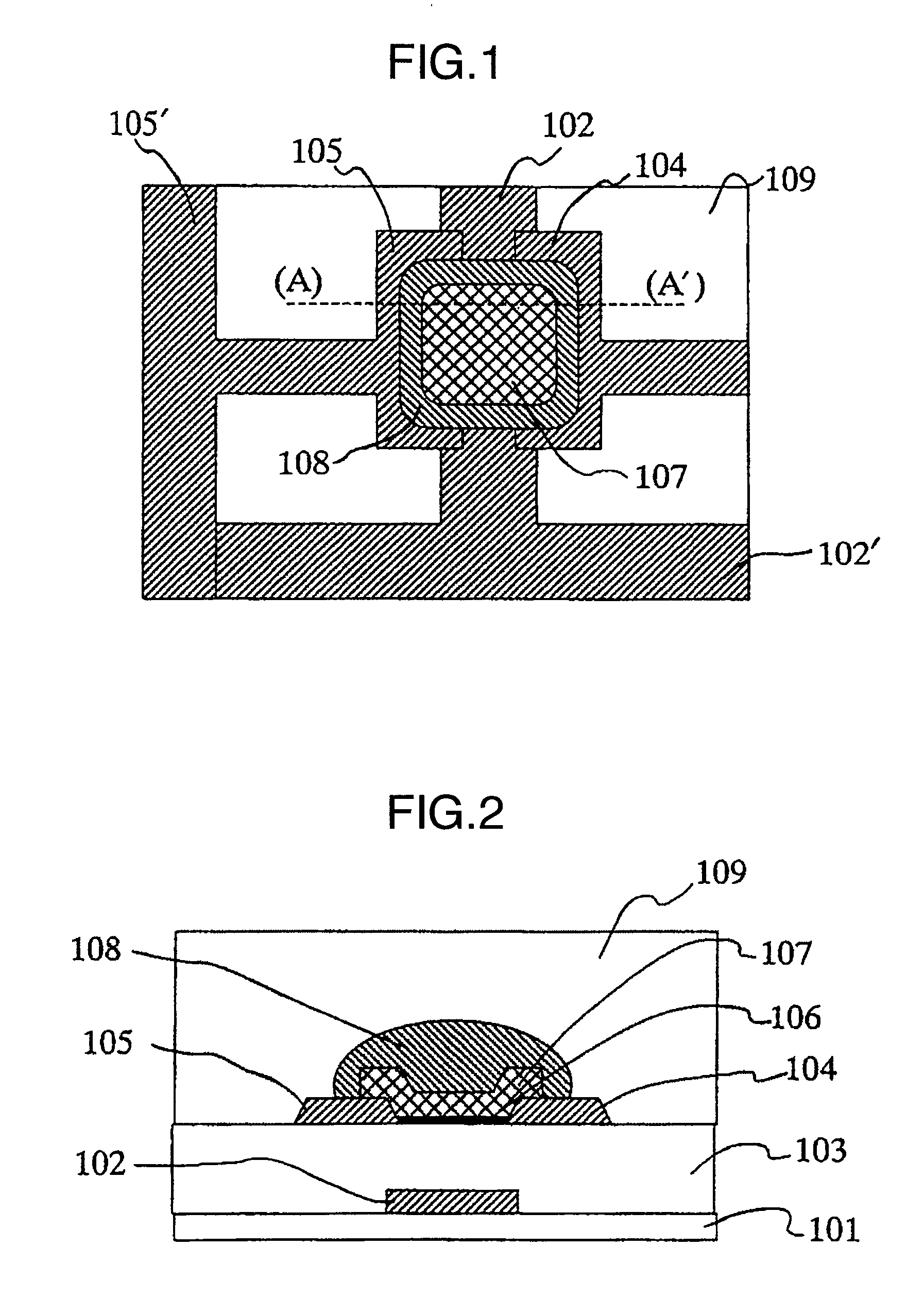
[0061]The first example of the present invention is described with reference to FIG. 1 to FIG. 4. FIG. 1 shows the planar schematic view of the organic thin film transistor using the present invention, and FIG. 2 shows the sectional schematic view of the organic thin film transistor using the present invention. FIG. 2 shows the section of (A)-(A′) in FIG. 1.

[0062]A glass substrate was used as the dielectric substrate 101. The dielectric substrate 101 can be selected from a broad range of dielectric materials. Specifically there can be used inorganic substrates such as quartz, sapphire, silicon and the like; and organic plastic substrates such as acrylic, epoxy, polyamide, polycarbonate, polyimide, polynorbornene, polyphenylene oxide, polyethylene naphthalenedicarboxylate, polyethylene terephthalate, polyethylene naphthalate, polyarylate, polyether ketone, polyether sulfone, polyketone, polyphenylene sulfide and the like. In addition, a film such as silicon oxide, silicon nitride or ...

example 2

[0071]The second example of the present invention is described with reference to FIG. 5. FIG. 5 shows the sectional schematic view of the organic thin film transistor using the present invention. A glass substrate was used as the dielectric substrate 101. The dielectric substrate 101 can be selected from a broad range of dielectric materials similarly to Example 1. Thereon were formed the gate electrode 102 and the scanning wiring 102′ of Cr at a thickness of 150 nm. The gate electrode 102 and the scanning wiring 102′ are not particularly limited as long as they are conductive materials, and can be selected from a broad range of materials similarly to Example 1. Next, as the gate dielectric layer 103, SiO2 film of 300 nm in thickness was formed by chemical vapor deposition. The gate dielectric layer 103 can be selected from a broad range of dielectric materials similarly to Example 1. Next, the surface of the above gate dielectric layer was modified with the monomolecular layer 106 ...

example 3

[0075]The third example of the present invention is described with reference to FIG. 6. FIG. 6 shows the sectional schematic view of the organic thin film transistor using the present invention. A glass substrate was used as the dielectric substrate 101. The dielectric substrate 101 can be selected from a broad range of dielectric materials similarly to Example 1. Thereon were formed the source electrode 104 / drain electrode 105 and signal wiring 105′ of Au at a thickness of 50 nm. The materials of source electrode 104 / drain electrode 105 and signal wiring 105′ are not particularly limited as long as they are conductive materials, and can be selected from a broad range of materials similarly to Example 1. Next, a soluble pentacene derivative was applied by ink jet method and fired to form the semiconductor layer 107 of 100 nm in thickness. The semiconductor layer 107 can be selected from a broad range of materials similarly to Example 1.

[0076]Next, a polyvinyl alcohol, in which an az...


PUM

PropertyMeasurementUnit
thicknessaaaaaaaaaa
thicknessaaaaaaaaaa
thicknessaaaaaaaaaa

Abstract

The present invention aims at providing a high-performance semiconductor device such as display, IC tag, sensor or the like at a low cost by using an organic thin film transistor most members of which can be formed by printing, as a switching element. The present invention relates to a thin film transistor composed of members on a dielectric substrate, which are a gate electrode, a dielectric film, source / drain electrodes, and a semiconductor layer, wherein on said semiconductor layer there are formed at least two passivation films of a first passivation film capping said semiconductor layer to protect it and a second passivation film covering larger area than that of said first passivation film to protect all of said members.

Description

FIELD OF THE INVENTION[0001]The present invention relates to a thin film transistor having improved performances and a semiconductor device using the same. In particular, the present invention relates to a method for preventing deterioration and peeling of a semiconductor formed by use of application techniques and printing techniques.[0002]In accordance with advancement of informatization, attention has been paid to development of a thin and light electronic paper display in place of paper, an IC tag capable of identifying commercial products individually at once, or the like. Currently in these devices, a thin film transistor using amorphous silicon or polycrystalline silicon as a semiconductor is used as a switching element. However, in producing thin film transistors using these silicon type semiconductors, there are problems that production cost is high because of necessity of an expensive apparatus such as plasma chemical vapor deposition apparatus or sputtering apparatus and ...

Claims


Application Information

Patent Timeline
Patent Type & Authority Applications(United States)
IPC IPC(8): H01L29/786G02F1/1368G09F9/30H01L21/84H01L27/00H01L51/00H01L51/05H01L51/30H01L51/50H05B33/14
CPCH01L51/0541H01L51/107H01L51/0545H10K10/464H10K10/466H10K10/88
Inventor KAWASAKI, MASAHIROIMAZEKI, SHUJIANDO, MASAHIKOSEKIGUCHI, YOSHIFUMIHIROTA, SHOICHI
Owner HITACHI LTD
Why Eureka
Try Eureka