Solid electrolytic capacitor and production method thereof

a technology production method, which is applied in the manufacture of electrolytic capacitors, electrolytic capacitors, coatings, etc., can solve the problems of increasing the leakage current, the contact area is not large enough, and the capacity of solid electrolytic capacitor chips is not increased, so as to achieve stable production of thin solid electrolytics, less short-circuit failure, and less fluctuation in the shape of elements

Inactive Publication Date: 2010-04-29
MURATA MFG CO LTD
View PDF9 Cites 17 Cited by
  • Summary
  • Abstract
  • Description
  • Claims
  • Application Information

AI Technical Summary

Benefits of technology

[0065]The present invention enables to stably produce thin solid electrolytic capacitor elements suitable for laminated type solid electrolytic capacitors, showing less short-circuit failure and less fluctuation in the shape of element, which allows to increase the number of laminated capacitor elements in a solid electrolytic capacitor chip to make a capacitor having a high capacity, and having less fluctuation in equivalent series resistance.

Problems solved by technology

This makes it easy for pastes or the like to contact the dielectric oxide film layer directly, thus leading to an increase in leakage current.
Further, the number of capacitor elements that can be laminated on a solid electrolytic capacitor chip having a predetermined size is limited depending on the thickness of the capacitor element, so that it has been unsuccessful to increase the capacity of solid electrolytic capacitor chips.
Furthermore, an uneven thickness with which the conductive polymer is attached causes a decrease in a contact area between the laminated capacitor elements, so that there will arise a problem that the equivalent series resistance (ESR) of the solid electrolytic capacitor chip increases.

Method used


Image

  • Solid electrolytic capacitor and production method thereof
  • Solid electrolytic capacitor and production method thereof
  • Solid electrolytic capacitor and production method thereof

Examples


example 1

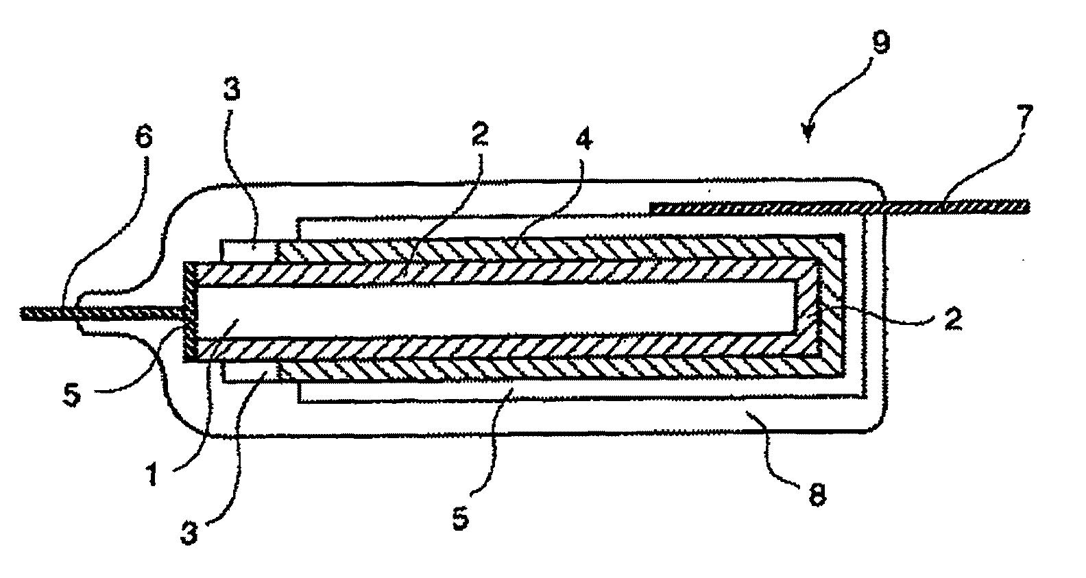
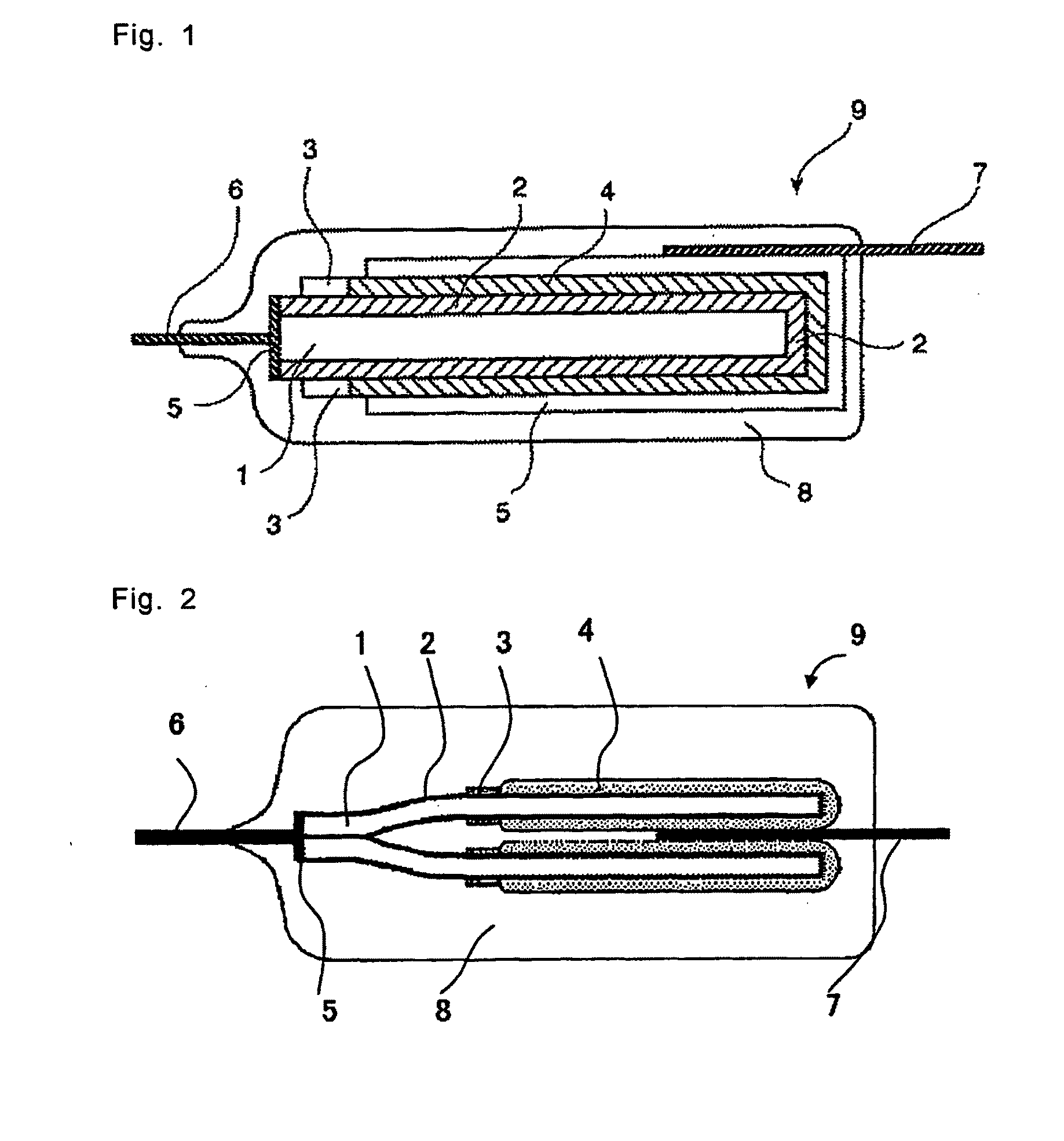
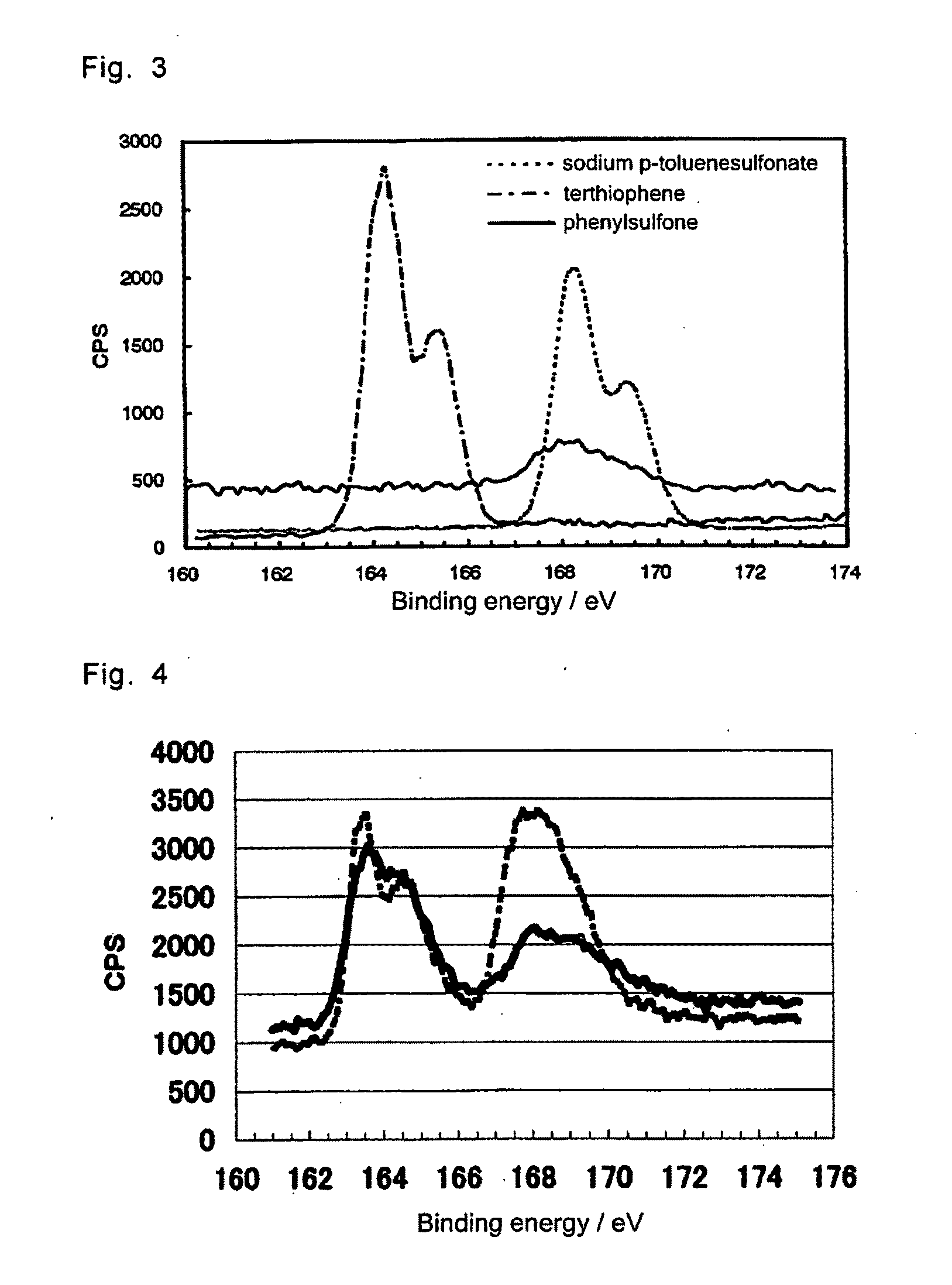
[0228]Chemically formed aluminum foil was cut to pieces of a size of 3.5 mm along short axis direction×11 mm along long axis direction. A polyimide solution was coated on both sides of the foil in a width of 1 mm circumferentially such that the foil is sectioned into two 5 mm portions along the long axis direction and dried to form masking. One of the portions the size of 3.5 mm×5 mm (cathode formed portion) of the chemically formed foil thus obtained was dipped in 10 mass % aqueous ammonium adipate solution and the cut portion was chemically formed by applying a voltage of 3.8 V to form a dielectric material oxide film. Then, the portion of the aluminum foil thus treated was dipped in Conductive Composition 1 for 5 seconds and dried at room temperature for 5 minutes. The spectrum showing the S2p binding energy determined by measuring through X-ray photoelectron spectroscopy (XPS) the surface of the dielectric layer provided on a layer having fine pores in the chemically-formed alum...

example 2

[0233]One of the portions the size of 3.5 mm×5 mm (cathode formed portion) of the chemically formed aluminum foil wherein a masking was provided in the same way as in Example 1 was treated in the same way as in Example 1 and the cut portion thereof was chemically formed to form a dielectric oxidized film. Then the chemically formed portion was dipped in Conductive Composition 1 for 5 seconds and dried at room temperature for 5 minutes and then dehydrocondensation reaction was performed at 300° C. for 15 minutes to allow crosslinking to proceed to form a self-doping type conductive polymer with the polymer chains thereof being crosslinked therebetween on a surface of the dielectric film (Step 1).

[0234]Further, a solid electrolyte was formed in the same manner as in Example 1 except that this operation was repeated once again.

[0235]Then, re-chemical-forming, coating of carbon paste and silver paste, lamination, connection of cathode lead terminal, sealing with epoxy resin, and aging o...

example 3

[0236]One of the portions the size of 3.5 mm×5 mm (cathode formed portion) of the chemically formed aluminum foil wherein a masking was provided in the same way as in Example 1 was treated in the same way as in Example 1 and the cut portion thereof was chemically formed to form a dielectric oxidized film. Then total 30 capacitors were completed in the same manner as in Example 1 except that a chemically formed aluminum foil was dipped in Conductive Composition 2 for 5 seconds and dried at room temperature for 5 minutes and then dehydrocondensation reaction was performed at 250° C. for 30 minutes to allow crosslinking to proceed to form a self-doping type conductive polymer with the polymer chains thereof being crosslinked therebetween on a surface of the dielectric film. The obtained capacitor elements were subjected to evaluation of characteristics in the same manner as in Example 1. Tables 1 and 2 show the results.


PUM

PropertyMeasurementUnit
binding energyaaaaaaaaaa
thicknessaaaaaaaaaa
electric conductivityaaaaaaaaaa

Abstract

The present invention relates to a solid electrolytic capacitor comprising a layer of self-doping type conductive polymer having a crosslink between polymer chains thereof on the dielectric film formed on a valve-acting metal. The present invention enables to stably produce thin capacitor elements suitable for laminated type solid electrolytic capacitors, showing less short-circuit failure and less fluctuation in the shape of element, which allows to increase the number of laminated elements in a solid electrolytic capacitor chip to make a capacitor having a high capacity, and having less fluctuation in equivalent series resistance.

Description

CROSS REFERENCE TO THE RELATED APPLICATIONS[0001]This is an application filed pursuant to 35 U.S.C. Section 111(a) with claiming the benefit of U.S. Provisional Application Ser. No. 60 / 695,541 filed Jul. 1, 2005 and No. 60 / 719,172 filed Sep. 22, 2005 under the provision of 35 U.S.C. Section 111(b), pursuant to 35 U.S.C. Section 119(e)(1).TECHNICAL FIELD[0002]The present invention relates to a solid electrolytic capacitor containing an electroconductive polymer on a dielectric film and to a method of producing the same.BACKGROUND ART[0003]Generally, as shown in FIG. 1, for example, fundamental elements of a solid electrolytic capacitor are fabricated by forming a dielectric oxide film layer (2) on each side of an anode substrate (1) made of an etched metal foil having a relatively large specific surface area, forming solid semiconductor layers (hereinafter, referred to as “solid electrolytes”) (4) as opposite electrodes on both sides of the dielectric oxide film layer (2), and prefer...

Claims


Application Information

Patent Timeline
Patent Type & Authority Applications(United States)
IPC IPC(8): H01G9/025
CPCC08G61/126H01G9/042H01G9/028H01G9/0036
Inventor SAIDA, YOSHIHIROFUKUNAGA, HIROFUMI
Owner MURATA MFG CO LTD
Why Eureka
Try Eureka