Photosensor and display device

a technology of display device and photosensor, which is applied in the field of photosensors, can solve the problems of low mobility of amorphous silicon thin film, high cost and impracticality of the size of an area sensor is limited by the size of a single crystal silicon substrate, so as to achieve low cost and impracticality, and the effect of high writing speed

Active Publication Date: 2010-06-03
SEMICON ENERGY LAB CO LTD
View PDF101 Cites 168 Cited by
  • Summary
  • Abstract
  • Description
  • Claims
  • Application Information

AI Technical Summary

Benefits of technology

[0030]According to the present invention, a large area sensor or a large line sensor can be provided which can convert intensity distribution of light received by a plurality of photoelectric conversion elements into electrical signals with high reproducibility and output the electrical signals. In addition, a display device with a high writing speed and little display unevenness which can also serve as a large area sensor which can convert intensity distribution of light received by photoelectric conversion elements arranged in a matrix into electrical signals with high reproducibility and output the electrical signals can be provided.

Problems solved by technology

An amplifier circuit including a single crystal silicon transistor has excellent characteristics; however the size of an area sensor is limited by the size of the single crystal silicon substrate.
In other words, formation of a large area sensor or a large area sensor also serving as a display device using a single crystal silicon substrate is costly and impractical.
However, field-effect mobility of an amorphous silicon thin film is low; thus, it is difficult to reduce an area occupied by the amplifier circuit.
If amplifier circuits including thin film transistors which vary in their characteristics are used, it is impossible to convert intensity distribution of light received by photoelectric conversion elements arranged in a matrix into electrical signals with high reproducibility and output the electrical signals.

Method used


Image

  • Photosensor and display device
  • Photosensor and display device
  • Photosensor and display device

Examples


embodiment 1

[0051]In this embodiment, an example of an area sensor including a plurality of photoelectric conversion elements and amplifier circuits is described with reference to drawings. The amplifier circuit includes thin film transistors including an oxide semiconductor, particularly, an oxide semiconductor containing indium, gallium, and zinc.

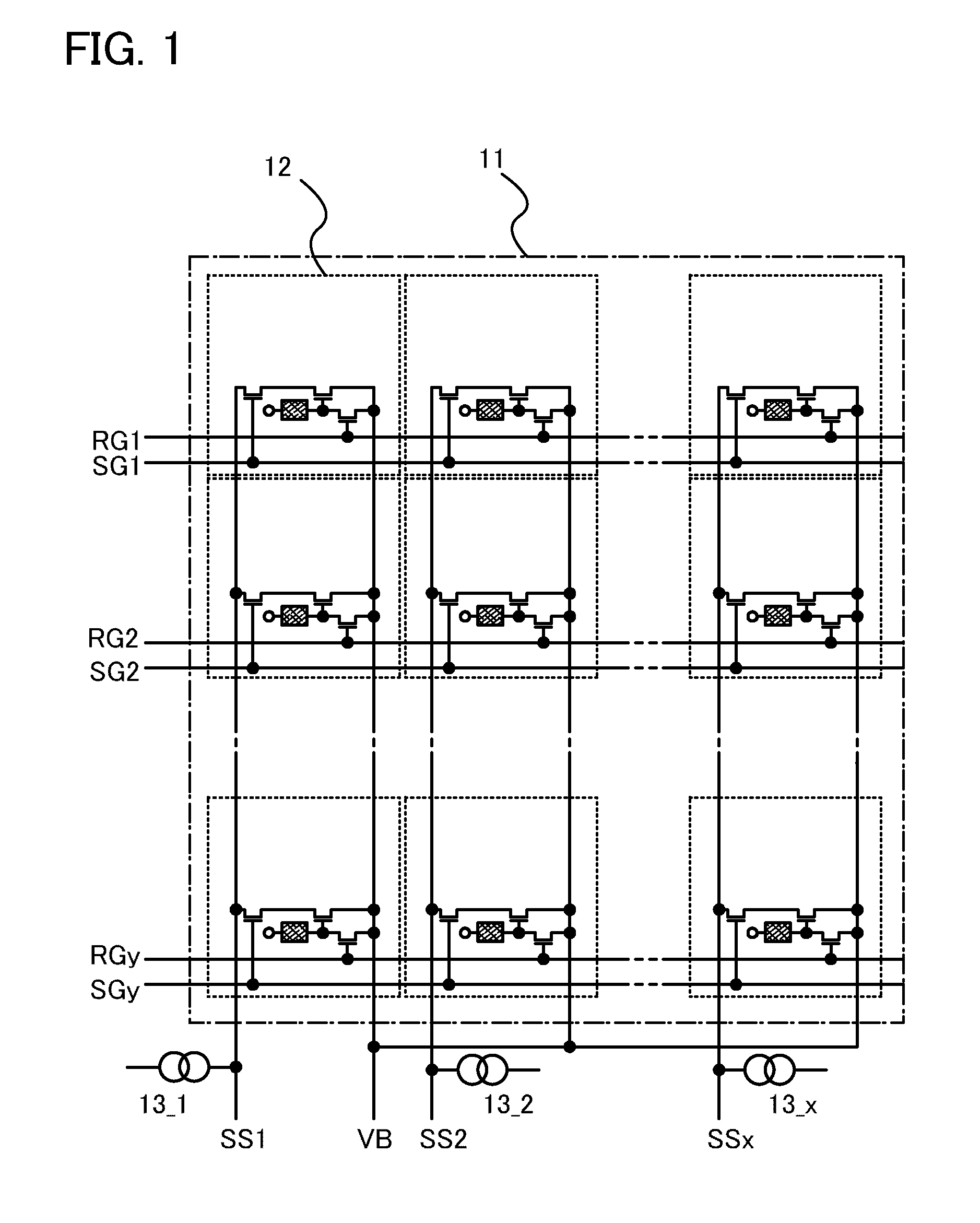
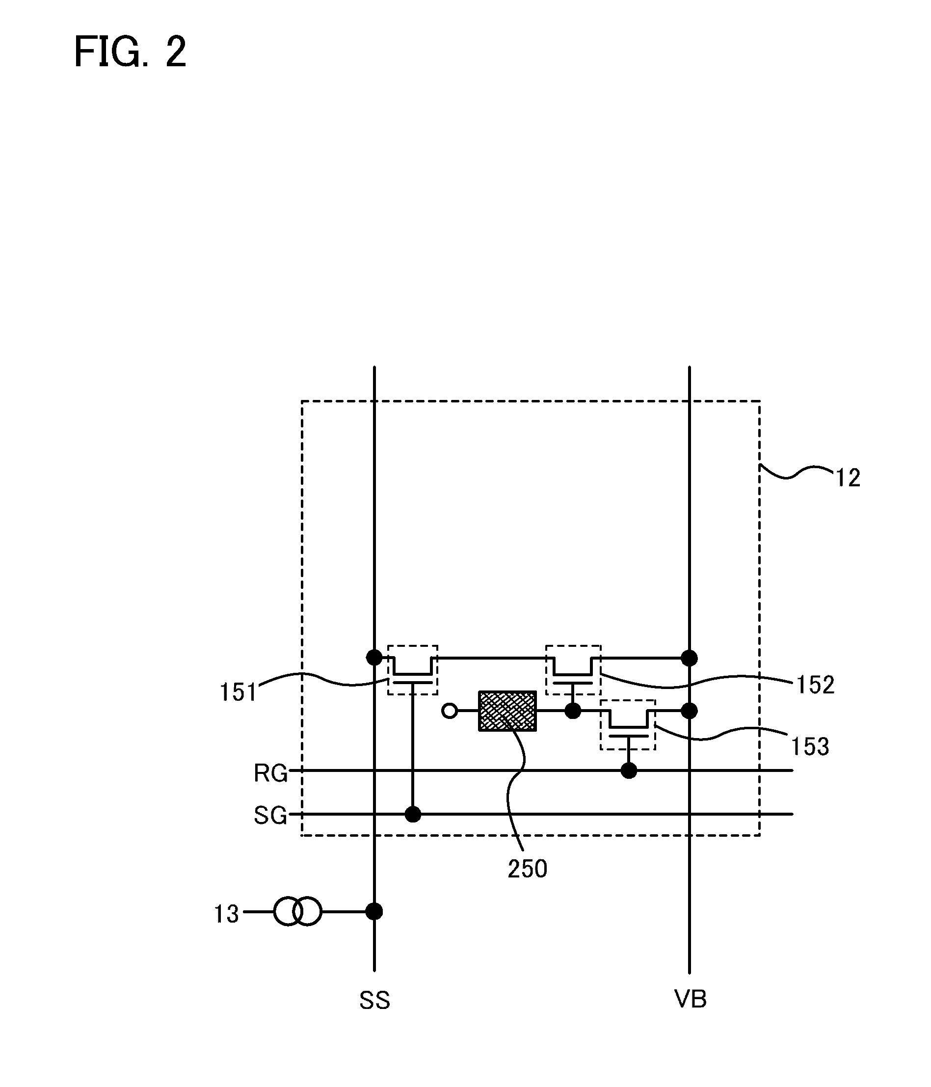
[0052]FIG. 1 illustrates connections of reset gate signal lines RG1 to RGy, sensor gate signal lines SG1 to SGy, sensor output wirings SS1 to SSx, a sensor power supply line VB, and a plurality of pixels 12 which are included in an area sensor portion 11.

[0053]In the area sensor portion 11, the plurality of pixels 12 are arranged in a matrix. Each of the pixels 12 is connected to one of the reset gate signal lines RG1 to RGy, one of the sensor gate signal lines SG1 to SGy, one of the sensor output wirings SS1 to SSx, and the sensor power supply line VB.

[0054]The sensor output wirings SS1 to SSx are connected to constant current power supplies 13_1 to...

embodiment 2

[0095]In this embodiment, an example of a manufacturing process for the area sensor in FIG. 4 which is described in Embodiment 1 is described with reference to FIGS. 5A to 5D and FIGS. 6A to 6D. Note that since main parts of the selection TFT 151, the amplifying TFT 152, and the reset TFT 153, the manufacturing process of which is described with reference to FIGS. 5A to 5D and FIGS. 6A to 6D, have the same structure, a process for forming the selection TFT 151 is mainly described below.

[0096]In FIG. 5A, a light-transmitting substrate is used as a substrate 100. A glass substrate of barium borosilicate glass, aluminoborosilicate glass, aluminosilicate glass, or the like available in the market can be employed. For example, a glass substrate which includes more barium oxide (BaO) than boric acid (B2O3) in composition ratio and whose strain point is 730° C. or higher is preferable. This is because such a glass substrate is not strained even when an oxide semiconductor layer is thermall...

embodiment 3

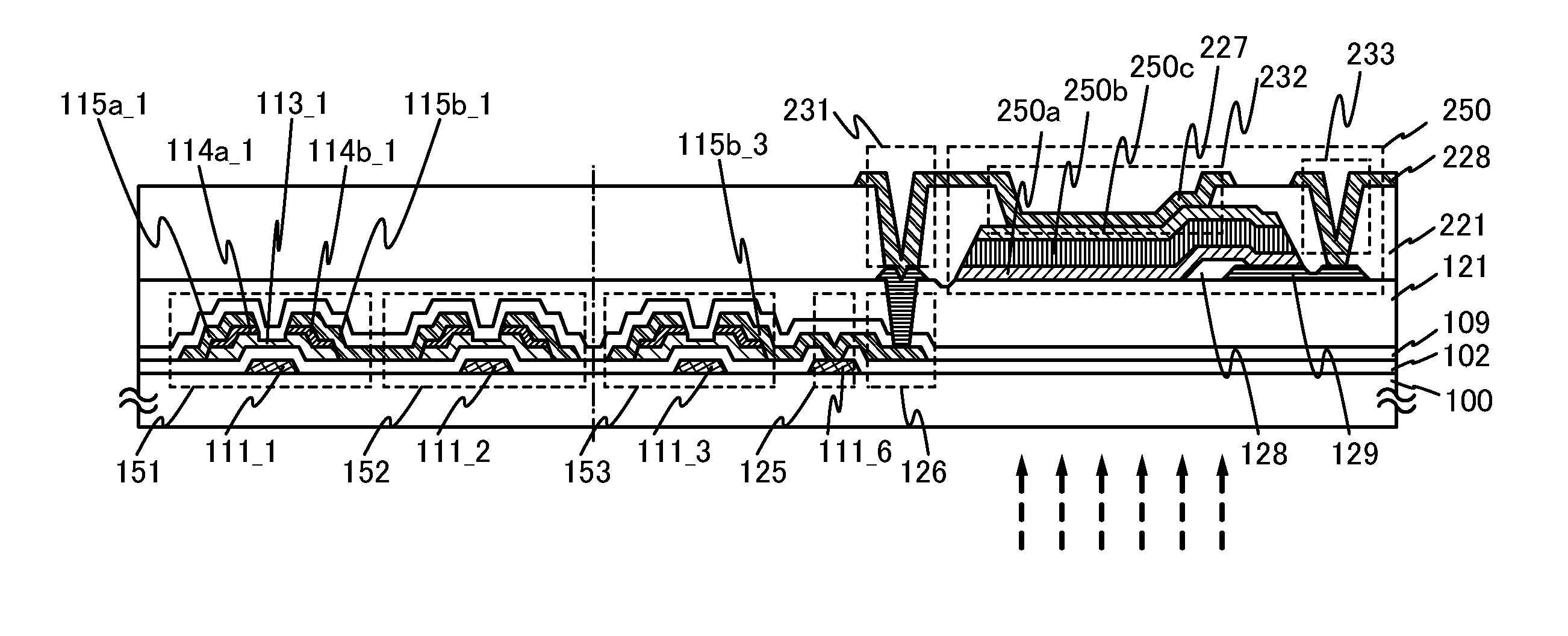
[0149]In this embodiment, a manufacturing process for an embodiment of an area sensor which is different from that of Embodiment 2 is described with reference to FIGS. 7A to 7D. In this embodiment, light directly reaches an area sensor which is formed over a substrate.

[0150]By the method described in Embodiment 2, an amplifier circuit which includes a thin film transistor including an oxide semiconductor containing indium, gallium, and zinc, the first interlayer insulating film 109, and the second interlayer insulating film 121 are formed over the substrate using four photomasks. FIG. 7A shows a cross-sectional view at this step. Note that if a structure in which light directly reaches the area sensor formed over the substrate is employed, the substrate 100, the gate insulating film 102, the first interlayer insulating film 109, and the second interlayer insulating film 121 are not always required to have a light-transmitting property. Further, the second interlayer insulating film ...


PUM

PropertyMeasurementUnit
temperatureaaaaaaaaaa
electrical conductivityaaaaaaaaaa

Abstract

Thin film transistors including an oxide semiconductor containing indium, gallium, and zinc are easily arranged in a matrix over a large substrate and have small characteristic variations. With amplifier circuits and driver circuits of display elements which include the thin film transistors including an oxide semiconductor containing indium, gallium, and zinc with small characteristic variations, intensity distribution of light received by the photodiodes arranged in a matrix is converted into electrical signals with high reproducibility and output, and the display elements arranged in a matrix can be uniformly driven.

Description

BACKGROUND OF THE INVENTION[0001]1. Field of the Invention[0002]The present invention relates to a photosensor. In particular, the present invention relates to a photosensor which include thin film transistors with high field-effect mobility and small characteristic variations and a photoelectric conversion element. Further, the present invention relates to a line sensor or an area sensor in which a plurality of pixels including the photosensor are arranged. Further, the present invention relates to a display device including the photosensor.[0003]2. Description of the Related Art[0004]In recent years, an image sensor including a photoelectric conversion element such as a diode, a CCD, and a CMOS which can read out an electrical signal having image information from an optical signal of image information or text or graphics on paper has been used.[0005]A line sensor and an area sensor are image sensors including a plurality of photoelectric conversion elements. A line sensor includes...

Claims


Application Information

Patent Timeline
Patent Type & Authority Applications(United States)
IPC IPC(8): G02F1/133H01L29/12H01L33/00H01L31/112G02F1/1333G02F1/1368H01L21/28H01L21/336H01L21/768H01L27/146H01L29/417H01L29/423H01L29/49H01L29/786H01L31/10H01L51/50H05B33/12
CPCG02F2001/13312H01L27/1225H01L31/1055H01L27/3234H01L27/323G02F1/13312H10K59/65H10K59/40H01L29/7869
Inventor NAKAMURA, YASUOTANADA, YOSHIFUMI
Owner SEMICON ENERGY LAB CO LTD
Why Eureka
Try Eureka