Photovoltaic Cell and Production Thereof

a photovoltaic cell and photovoltaic technology, applied in the direction of photovoltaic energy generation, basic electric elements, electrical apparatus, etc., can solve the problems of limited use of photovoltaic cells, general neglect of current, and a number of drawbacks of methods, so as to reduce surface metal contacts, good efficiency, and good absorption

Inactive Publication Date: 2010-08-05
BP SOLAR ESPANA UNIPERSONAL
View PDF3 Cites 39 Cited by
  • Summary
  • Abstract
  • Description
  • Claims
  • Application Information

AI Technical Summary

Benefits of technology

[0021]The inventors of the present invention have surprisingly found that the benefits of using a deep groove grid, can be combined with that of reduced surface metal contacts, to produce an alternative photovoltaic cell having good efficiency, and good absorption in both the blue-violet portion of the spectrum and the red-infared portion.

Problems solved by technology

However their use is limited by their electrical output Typically, many photovoltaic cells are arranged in one or more panels or modules in order to generate sufficient power required for a desired commercial or consumer application.
However, this current is generally neglected in the standard solar cell since there is a high concentration of impurities, which act to produce a minimum of electron-hole pairs that recombine at the junction.
However, such a method suffers from a number of drawbacks.
Current production technologies providing required manufacturing yields add excessive cost in terms of raw material consumption and long cycle time to the process far preparing the solar cell.
In addition, a problem associated with the electroless plating process is that it prevents the formation of a uniform well defined back-surface field, and the benefits associated therewith.
Conversely, achieving a uniform well defined back surface field, such as using thick Aluminum films in the rear, would result in poor metallization yield which in turn affects detrimentally the performance of the solar cell.

Method used


Image

  • Photovoltaic Cell and Production Thereof
  • Photovoltaic Cell and Production Thereof
  • Photovoltaic Cell and Production Thereof

Examples


Embodiment Construction

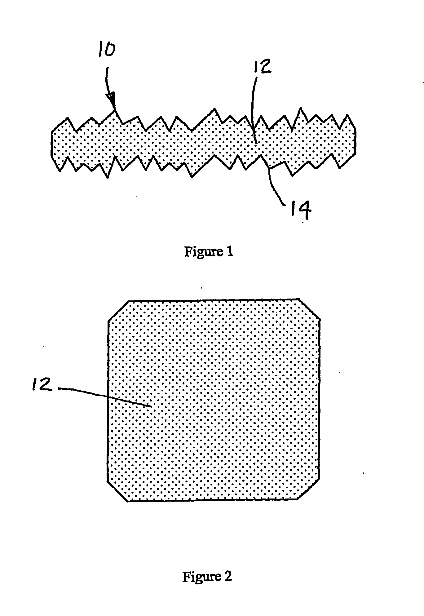
[0085]FIG. 1 shows a cross-section of a cell 10 in accordance with an embodiment of this invention. The photovoltaic cell 10 comprises a textured substrate, for example p-doped With boron, 12. The texture is symbolically depicted as 14.

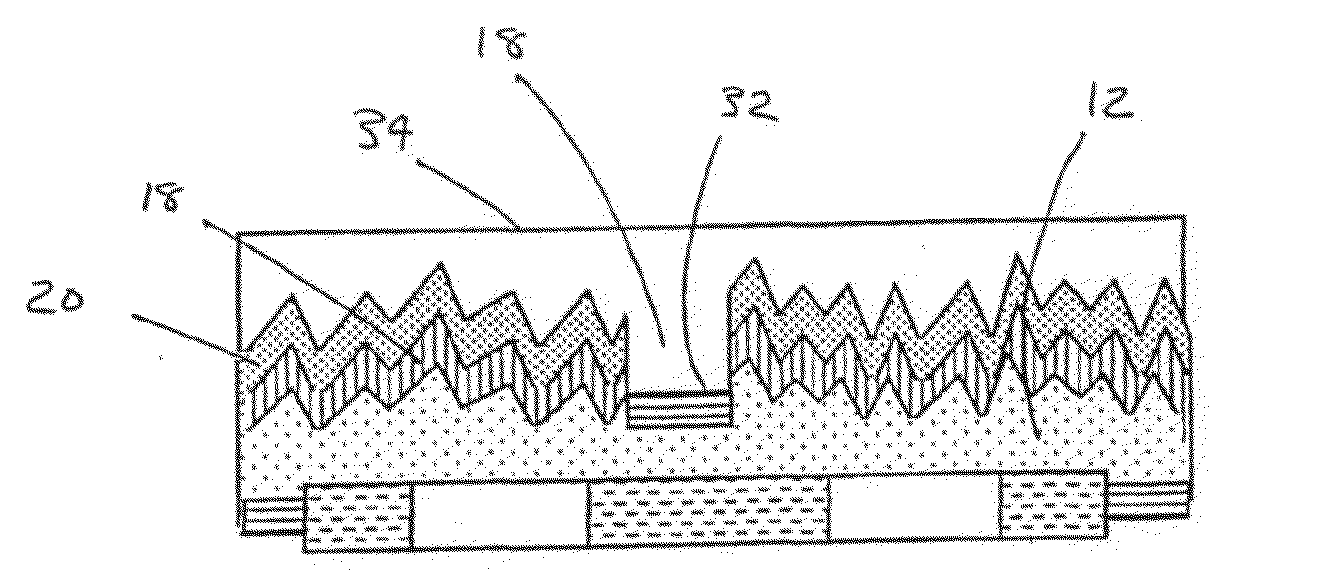
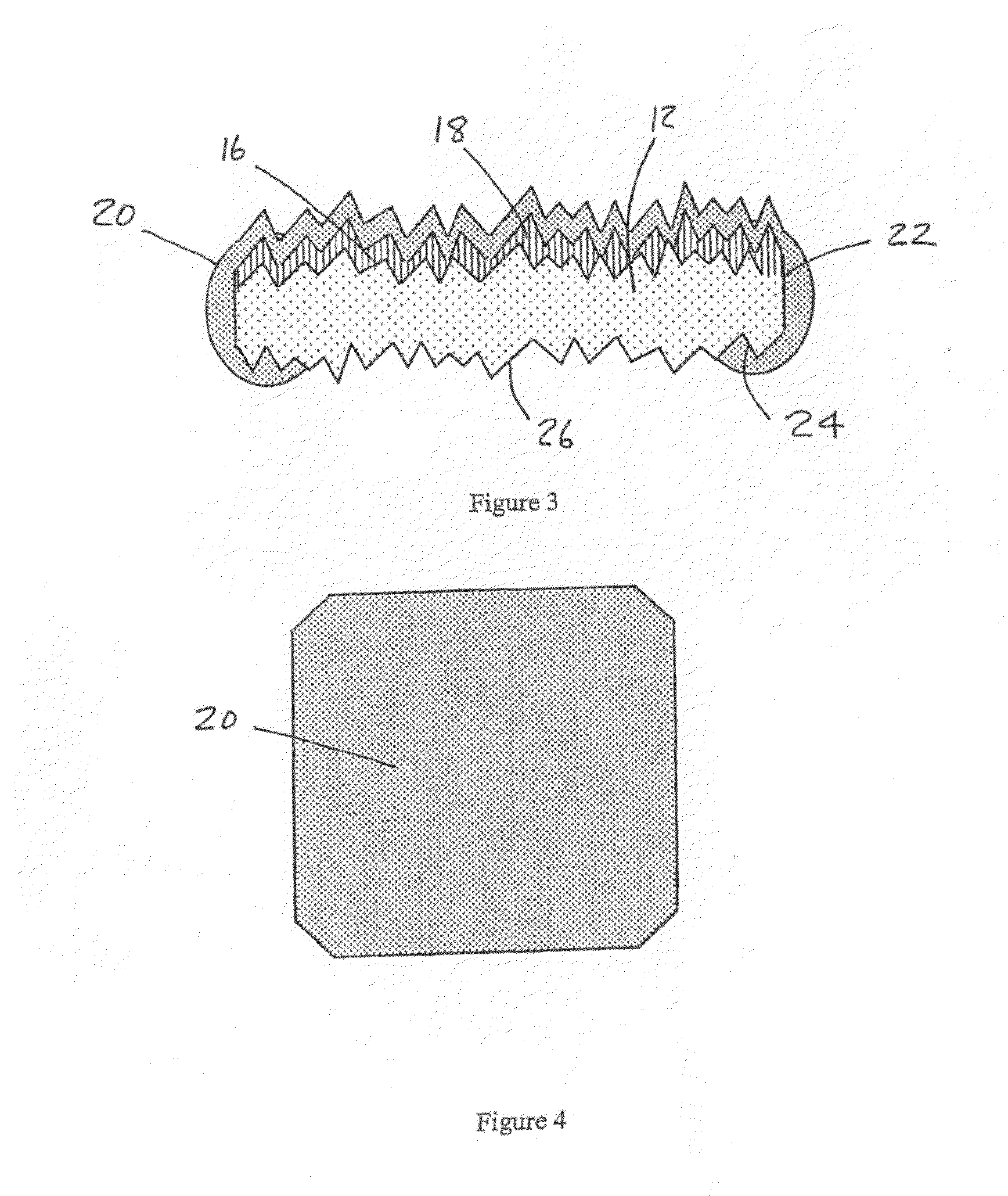
[0086]In FIG. 3, a textured, n-doped first layer 18, formed by, for example, phosphorus diffusion, is present on the front surface 16, of the substrate 12, producing a p-n junction where the boron doped substrate 12 meets the n-doped layer 18. A second surface coating 20 is disposed over the first layer 18 of the cell on the edges 22, the front surface 16, and the periphery 24 of the back surface 26.

[0087]After forming the first layer 18, and second surface coating 20, the device 10 is cleaned and etched (see FIG. 5) so as to remove unwanted parts of the coating 20.

[0088]As shown in FIG. 7, grooves 28 are formed in the substrate 12, through the layer 18 and surface coating 20. After forming the grooves 28, a cleaning process is undertaken so as to rem...


PUM

PropertyMeasurementUnit
thickaaaaaaaaaa
thickaaaaaaaaaa
thickaaaaaaaaaa

Abstract

A process for producing a photovoltaic device having a substrate comprising silicon doped with a first dopant, the process comprising the steps of: a. forming a first layer over a front surface of the substrate, the first layer comprising a second dopant of a conductivity type opposite the first dopant; b. forming a second surface coating over the first layer; c. forming elongate grooves reaching or entering the silicon substrate, d. forming a third layer within the grooves, the layer comprising a third dopant of a conductivity type opposite to the first dopant; e. forming a contact finger system which intersects with the grooves to provide an electrically conducting front contact; and f. forming a second contact.

Description

BACKGROUND OF THE INVENTION [0001]The present invention relates to photovoltaic devices, particularly photovoltaic devices comprising thin layers of semiconductor materials, such as thin layers of monocrystalline or multicrystalline silicon. More particularly, the present invention relates to photovoltaic devices comprising monocrystalline or multicrystalline silicon semiconductor materials.[0002]The photovoltaic devices, also known as photovoltaic cells, are used to convert light energy into electrical energy. Photovoltaic cells can be used to generate energy (solar cells) or they can be used as photodetector elements in other devices. Photovoltaic cells are a source of renewable energy. However their use is limited by their electrical output Typically, many photovoltaic cells are arranged in one or more panels or modules in order to generate sufficient power required for a desired commercial or consumer application.[0003]Photovoltaic cells having greater efficiency result In modul...

Claims


Application Information

Patent Timeline
Patent Type & Authority Applications(United States)
IPC IPC(8): H01L31/04H01L31/00H01L31/18H01L31/0216H01L31/068
CPCH01L31/022425H01L31/022433Y02E10/547H01L31/068H01L31/18H01L31/0236H01L31/02363
Inventor FERNANDEZ, JUAN M.BUENO, RAFAEL M.MORILLA, CARMENVINCUERIA, INES
Owner BP SOLAR ESPANA UNIPERSONAL
Why Eureka
Try Eureka