Bandgap engineered charge trapping memory in two-transistor nor architecture

a technology of charge trapping memory and bandgap, which is applied in the field of flash memory technology, can solve the problems of limiting the ability to increase the density of flash memory, affecting the performance of flash memory, so as to reduce power consumption and improve performance. the effect of programming

Active Publication Date: 2010-10-21
MACRONIX INT CO LTD
View PDF81 Cites 18 Cited by
  • Summary
  • Abstract
  • Description
  • Claims
  • Application Information

AI Technical Summary

Benefits of technology

[0021]In alternatives for both gate injection and channel injection embodiments, the control circuitry is arranged to induce channel hot electron programming. In alternatives of the channel hot electron programming devices, the access transistor can b

Problems solved by technology

As the density increases in memory devices, and the floating gate memory cells get closer and closer together, interference between the charge stored in adjacent floating gates becomes a problem.
This is limiting the ability to increase the density of flash memory based on floating gate memory cells.
However at that thickness, the endurance and charge retention characteristics of the memory cell are poor relative to traditional floating gate technology.
Also, with relatively thick tunneling dielectric layers, the electric field required for the erase operation also causes electron injection from the gate through the blocking dielectric layer.
However, if the erase saturation level is too high, the cell cannot be erased at all, or the threshold margin between the programmed and erased s

Method used


Image

  • Bandgap engineered charge trapping memory in two-transistor nor architecture
  • Bandgap engineered charge trapping memory in two-transistor nor architecture
  • Bandgap engineered charge trapping memory in two-transistor nor architecture

Examples


Embodiment Construction

[0059]A detailed description of embodiments of the present invention is provided with reference to the FIGS. 3-45.

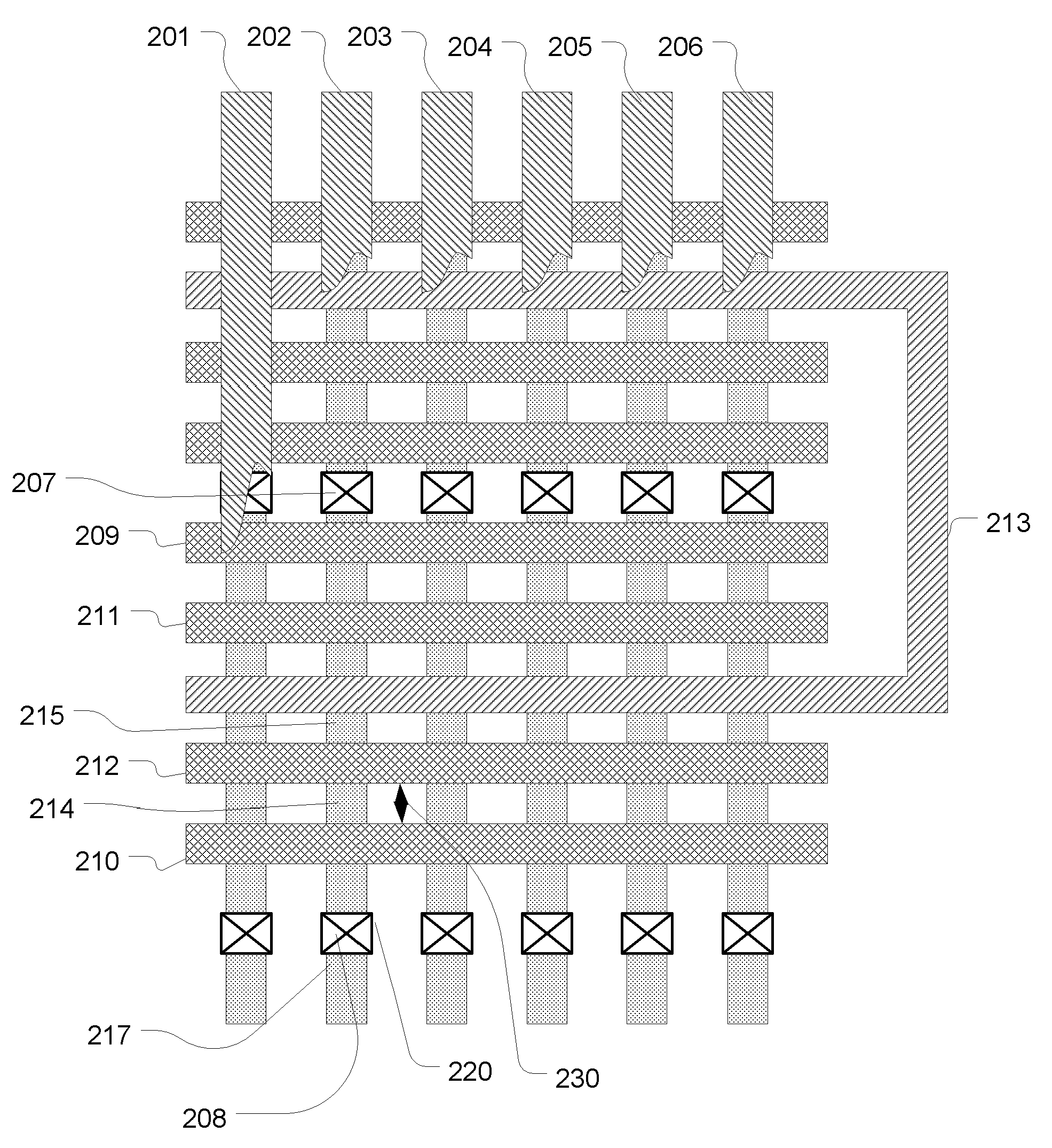
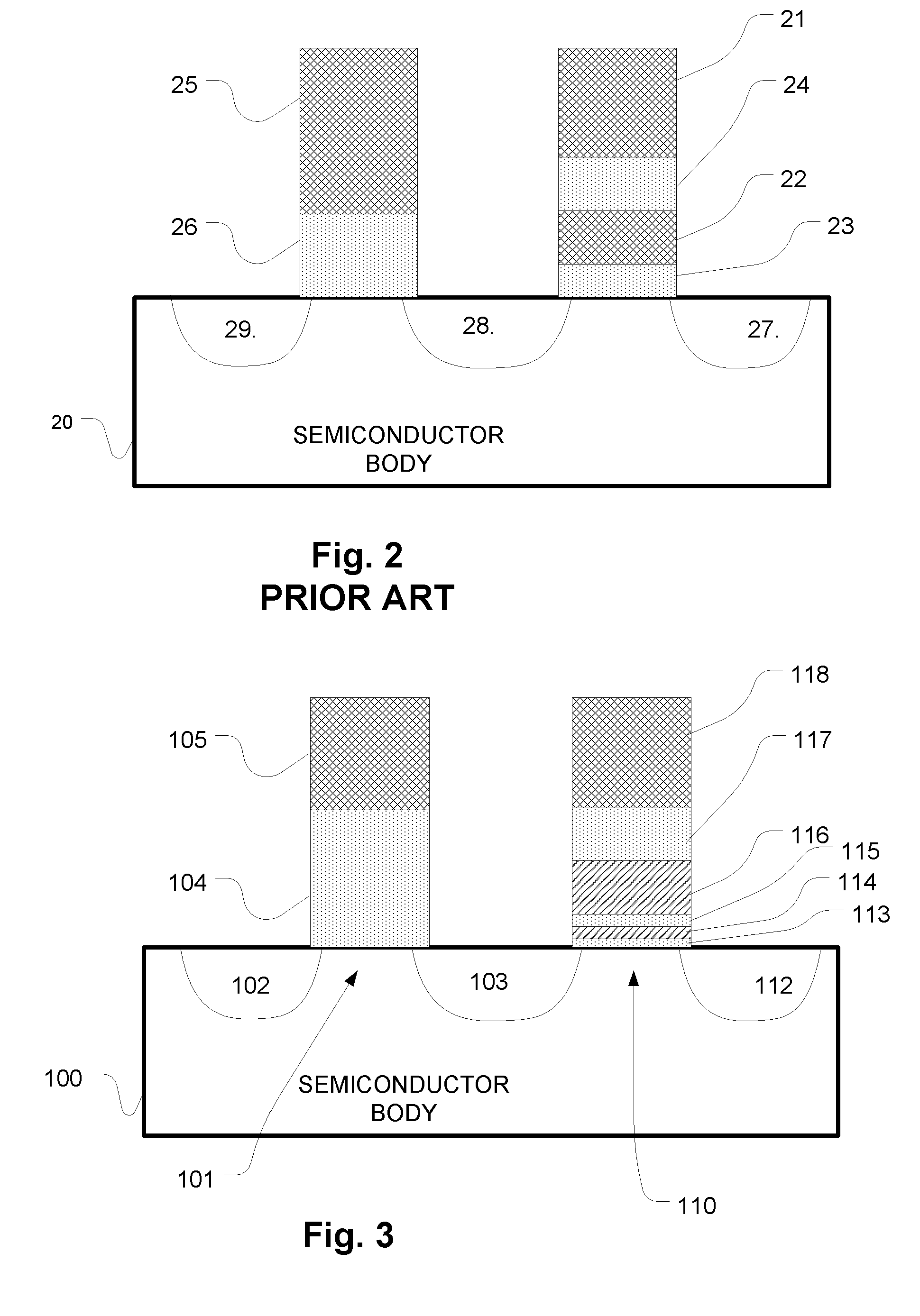
[0060]FIG. 3 is a simplified diagram of a 2T cell including charge trapping memory transistors employing a bandgap engineered dielectric tunneling layer. The memory cell is formed on a semiconductor body 100, and includes an access transistor and memory transistor. The access transistor includes a channel 101, a source 102 and a drain in terminal 103. A gate dielectric layer 104 overlies the channel 101, and a gate 105 overlies the gate dielectric 104. The memory transistor includes a channel 110, a source in terminal 103 and a drain 112 adjacent the channel. A gate 118 overlies a multilayer stack of dielectric materials acting as the charge storage structure, including a blocking dielectric layer, a charge trapping layer and a tunneling layer. In this example, the charge trapping layer is in contact with the tunneling layer, but can be otherwise disposed between the tun...


PUM


Abstract

A 2T cell NOR architecture based on the use of BE-SONOS for embedded memory includes memory cells having respective access transistors having access gates and memory transistors having memory gates arranged in series between the corresponding bit lines and one of the plural reference lines. A memory transistor in a memory cell comprises a semiconductor body including a channel having a channel surface and a charge storing dielectric stack between the memory gate and the channel surface. The dielectric stack comprises a bandgap engineered, tunneling dielectric layer contacting one of the gate (for gate injection tunneling) and the channel surface (for channel injection tunneling). The dielectric stack of the memory cell also includes a charge trapping dielectric layer on the tunneling dielectric layer and a blocking dielectric layer.

Description

BACKGROUND OF THE INVENTION[0001]1. Field of the Invention[0002]The present invention relates to flash memory technology, and more particularly to charge trapping memory technology adaptable for high speed erase and program operations and suitable for use as embedded memory in large scale integrated circuits.[0003]2. Description of Related Art[0004]Flash memory is a class of non-volatile integrated circuit memory technology. Traditional flash memory employs floating gate memory cells. As the density increases in memory devices, and the floating gate memory cells get closer and closer together, interference between the charge stored in adjacent floating gates becomes a problem. This is limiting the ability to increase the density of flash memory based on floating gate memory cells. Another type of memory cell used for flash memory can be referred to as a charge trapping memory cell, which uses a dielectric charge trapping layer in place of the floating gate. Charge trapping memory ce...

Claims


Application Information

Patent Timeline
IPC IPC(8): G11C16/02H01L29/792G11C16/06
CPCG11C16/0433H01L21/28282H01L29/513H01L27/11568H01L29/4234H01L27/11565H01L29/40117H10B43/10H10B43/30
Inventor LUE, HANG-TING
Owner MACRONIX INT CO LTD
Why Eureka
Try Eureka