Fabricating method of polycrystalline silicon thin film, polycrystalline silicon thin film fabricated using the same

a technology of polycrystalline silicon and thin film, which is applied in the direction of semiconductor devices, electrical devices, transistors, etc., can solve the problems of low aperture ratio, low mobility of electrons functioning as charge carriers, and inability to meet the requirements of cmos processes, and achieve excellent crystallinity and reduce processing time

Inactive Publication Date: 2010-10-28
ENSIL TECH CO LTD
View PDF1 Cites 9 Cited by
  • Summary
  • Abstract
  • Description
  • Claims
  • Application Information

AI Technical Summary

Benefits of technology

[0020]According to the present invention, a method of fabricating a polycrystalline silicon thin film which can ensure process stability at high temperature such as 1300° C. or more, thereby reducing processing time and obtaining a polycrystalline silicon thin film having excellent crystallinity, a polycrystalline silicon thin film fabricated using the same, and a thin film transistor including the polycrystalline silicon thin film are provided.

Problems solved by technology

Generally, amorphous silicon (a-Si) has disadvantages including low mobility of electrons functioning as charge carriers and a low aperture ratio, and other that makes it inappropriate for a CMOS process.
However, a polycrystalline silicon (poly-Si) thin film device enables a driving circuit required for writing an image signal in a pixel to be mounted on a substrate in the same manner as a pixel TFT-array, implementation of which was impossible with an a-Si TFT.
For high temperature processes, a substrate has to be formed of an expensive material such as quartz, and thus is not appropriate for a large display.
SPC enables a uniform crystal quality to be obtained using inexpensive equipment, but requires high crystallization temperature and long processing time, and thus, for example, a glass substrate having a relatively low heat deflection temperature cannot be used, and productivity is low.
Moreover, in SPC, twin-growth is observed during solid state phase transformation from an amorphous phase to a crystal phase, and thus contains many crystal lattice defects in formed grains.
However, in an actual process of fabricating a poly-Si TFT using MIC, these metals can cause serious contamination in a channel.
That is, it reduces metal contamination when compared to MIC, but does not completely overcome this problem.
FALC has a fast crystallization rate and anisotropy in crystallization direction when compared to MILC, but still does not overcome metal contamination.
MIC, MILC and FALC are all effective for a decrease in crystallization temperature compared to SPC, but all have common disadvantages of long crystallization time and crystallization induced by metal.
Thus, none of these techniques is free from metal contamination.
For example, these are problems of a laser system having non-uniform radiation amount of a laser beam, a laser process having an ultimately limited process region of a laser energy density for obtaining large grains, and a shot trace on a large display.
The first two problems cause non-uniformity in grain size of the poly-Si thin film constituting an active layer of the poly-Si TFT.
In addition, poly-Si produced along with phase transformation from a liquid state to a solid state undergoes volume expansion, and thus a severe protrusion phenomenon occurs to a surface from a place where a grain boundary is formed.
This phenomenon directly affects a gate insulating layer formed in a subsequent process, and thus reduces a breakdown voltage due to non-uniform planarization ratio at an interface between the poly-Si and the gate insulating layer and device reliability such as hot carrier stress.
While sequential lateral solidification (SLS) has been developed in recent times to solve the instability of ELC described above, thereby succeeding in stabilizing the process region of the laser energy density, it still does not overcome the problems of the shot trace and the protrusion phenomenon to the surface.
In view of the current trend of rapidly development of the flat panel display industry, technology for applying laser to a crystallization process for a substrate larger than 1 m×1 m, which is expected to be demanded for mass-production sooner or later, still has problems.
Moreover, equipment for ELC and SLS is very expensive, and thus high initial investment and maintenance are required.
Thus, the low temperature crystallization by ELC or SLS faces limits in the current flat panel display industries.
However, the Joule heating requires application of a higher electrical field to a conductive layer in a shorter period of time to shorten processing time.

Method used


Image

  • Fabricating method of polycrystalline silicon thin film, polycrystalline silicon thin film fabricated using the same
  • Fabricating method of polycrystalline silicon thin film, polycrystalline silicon thin film fabricated using the same
  • Fabricating method of polycrystalline silicon thin film, polycrystalline silicon thin film fabricated using the same

Examples


example 1

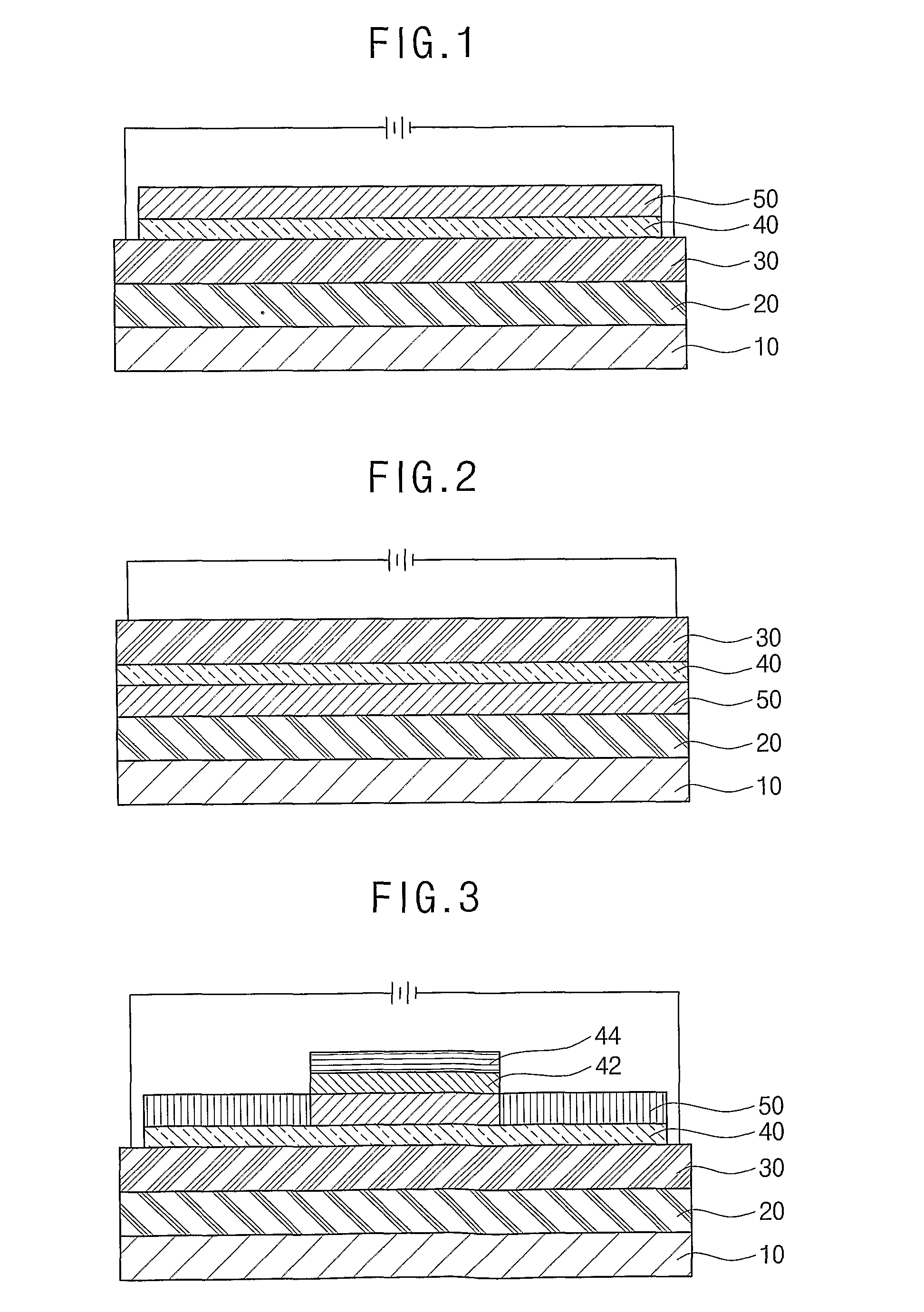
[0062]A 3000 Å SiO2 layer (a first insulating layer) was formed on a glass substrate with a size of 2 cm (L)×2 cm (W)×0.7 mm (H) by PECVD. A 1000 Å molybdenum (Mo) layer was deposited on the first insulating layer by sputtering, and a 1000 Å SiO2 layer (a second insulating layer) was then deposited by PECVD. A 500 Å a-Si thin film was deposited on the second insulating layer by PECVD, and thus a substrate including the a-Si thin film was completed as shown in FIG. 1. Here, the resistance of the Mo layer was 1.75Ω.

[0063]A voltage of 280V / cm was applied to the Mo layer of the sample described above for 300 μs. In the application of the electrical field, an energy content applied to the Mo layer was about 20000 Watt / cm2, and instantaneous temperature was increased to 1350° C.

example 2

[0064]A 3000 Å SiO2 layer (a first insulating layer) was formed on a glass substrate with a size of 2 cm (L)×2 cm (W)×0.7 mm (H) by PECVD. A 1000 Å titanium (Ti) layer was deposited on the first insulating layer by sputtering, and a 1,000 Å SiO2 layer (a second insulating layer) was then deposited by PECVD. A 500 Å a-Si thin film was deposited on the second insulating layer by PECVD, and thus a substrate including the a-Si thin film was completed as shown in FIG. 1. Here, the resistance of the Ti layer was 7.5Ω.

[0065]A voltage of 500V / cm was applied to the Ti layer of the sample described above for 300 μs. In the application of the electrical field, the energy content applied to the Ti layer was about 19000 Watt / cm2, and the instantaneous temperature was increased to 1300° C.


PUM

PropertyMeasurementUnit
melting pointaaaaaaaaaa
temperatureaaaaaaaaaa

Abstract

Provided are a method of fabricating a polycrystalline silicon thin film using high temperature heat generated by Joule heating induced by application of an electrical field to a conductive layer, which can ensure process stability at high temperature and thus processing time can be reduced and a polycrystalline silicon thin film having excellent crystallinity can be obtained, a polycrystalline thin film using the method and a thin film transistor including the polycrystalline thin film. The method includes providing a substrate, forming a metal or metal alloy layer having a melting point of 13000 C or more on the substrate, forming an insulating layer on the metal or metal alloy layer, forming an amorphous silicon (a-Si) thin film, an amorphous/polycrystalline composite silicon thin film, or a poly-Si thin film on the insulating layer, and applying an electrical filed to the metal or metal alloy layer to induce Joule heating and generate high temperature heat, and crystallizing and annealing the amorphous silicon (a-Si) thin film, the amorphous/polycrystalline composite silicon thin film, or the poly-Si thin film using the high temperature heat.

Description

TECHNICAL FIELD[0001]The present invention relates to a method of fabricating a polycrystalline silicon thin film, a polycrystalline thin film fabricated using the method, and a thin film transistor including the polycrystalline silicon thin film. More particularly, the present invention relates to a method of fabricating a polycrystalline silicon thin film using Joule heat generated by applying an electrical field to a conductive layer, the method using a metal or metal alloy layer having a melting point of 1300° C. or more as the conductive layer to ensure process stability at high temperature, thereby reducing processing time and obtaining a polycrystalline silicon thin film having excellent crystallinity, a polycrystalline silicon thin film fabricated by the method, and a thin film transistor (TFT) including the polycrystalline silicon thin film.BACKGROUND ART[0002]Generally, amorphous silicon (a-Si) has disadvantages including low mobility of electrons functioning as charge car...

Claims


Application Information

Patent Timeline
Patent Type & Authority Applications(United States)
IPC IPC(8): H01L29/786H01L21/336
CPCH01L21/02381H01L21/02422H01L21/02425H01L21/02488H01L21/02491H01L27/1281H01L21/02595H01L21/02667H01L29/66757H01L29/78603H01L21/02502H01L21/326
Inventor RO, JAE-SANGHONG, WON-EUI
Owner ENSIL TECH CO LTD
Why Eureka
Try Eureka