

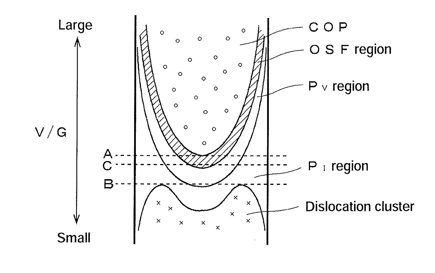
Silicon wafer and method for producing the same
a technology of silicon wafers and silicon chips, applied in the field of silicon wafers, can solve the problems of defective device characteristics, large amount of interstitial silicon, and adverse influence of device characteristics
- Summary
- Abstract
- Description
- Claims
- Application Information
AI Technical Summary
Benefits of technology
Problems solved by technology
Method used
Image

Examples
examples
[0080]A wafer consisting of defect-free regions was subjected to an RTP in an oxidizing atmosphere, and the wafer after this processing was examined for the density of the grown-in defects including silicon oxides. For comparison, a wafer subjected to the RTP in an Ar gas atmosphere and a wafer without the RTP were similarly examined.
[0081]A wafer used for the examination was cut out of a single crystal silicon ingot consisting of defect-free regions as being free of COPs and dislocation clusters, which is grown by the CZ method. Two classes of wafers that have interstitial oxygen concentrations of 12.0×10¹⁷ atoms / cm3 (wafer level 1) and 9.1×10¹⁷ atoms / cm3 (wafer level 2) respectively were used.
[0082]A lamp anneal furnace was used for the RTP, and an atmosphere of 100% of oxygen or 100% of Ar (Comparative Example) is maintained in the furnace. The processing temperature and duration time were each 1,250° C. and 10 seconds.
[0083]In the vicinity of the wafer surface layer after the RT...
PUM
 Abstract
Description
Claims
Application Information