
Unified scalable high speed interconnects technologies

Inactive Publication Date: 2010-12-09
WAYMO LLC
View PDF45 Cites 127 Cited by
  • Summary
  • Abstract
  • Description
  • Claims
  • Application Information

AI Technical Summary

Benefits of technology

[0019]The invention, in several embodiments, described here pertains to the field of high speed digital transmission across an array of subsystems. Furthermore, the basic Periodic Micro Coaxial Transmission Line (PMTL) described here can provide Confined Field Interconnection (CFI) between devices in wafer and on a high speed board, thus practically eliminating cross talk and parasitic, and allowing much higher speeds and wider bandwidth. An expansion of the idea of PMTL has been made by introducing of Vertical Micro Transmission Line VMTL using a array of 3D vias PTH and NPTH to provide true 3d signal flow with highest signal integrity. Throughout this disclosure, PTH refers to Plated Through Hole, and NPTH refer to via holes not plated, and either left empty of filled with air / gases or other materials.
[0027]It is a well-known fact that one of the major impediments to increasing signal speeds on copper transmission lines is the signal loss over frequency which exhibits a low pass filter characteristics. As previously mentioned, there are essentially two main mechanism of signal loss, conductor loss which varies as inverse of square root of frequency, and propagation losses which varies as inverse of frequency. Other secondary losses mechanism such as current bunching also effects losses. The inventions disclosed here provides techniques that help mitigates these losses and provide optimally low loss transmission line media that can be realized on CMOS or PCB, hard or soft, and at every level and hierarchy of fan out and fan in signal flow. A published report by Izadian has shown excellent performance from DC to 50 GHz of samples of several flexible PMTL transmission line in a series of measurements and evaluation data carried out by highly reliable Signal Integrity Laboratories. In addition, extensive Electromagnetic simulation suggests that the technology can work to THz frequencies with current state of the art manufacturing, and with process improvements to ultimately to light frequencies.
[0028]Perhaps, the best metal based TEM transmission line is the coaxial line. In a coaxial line, the near perfect TEM mode of propagation allows for low signal loss to great frequencies of nearly 500 GHz, for most practical application. But, the coaxial lines are usually manufactured by extrusion and are not very useful in PCB and COMS scales. The PMTL-VMTL however provides a means to achieve a nearly coaxial line transmission efficiencies but using CMOS or PCB processes, and promises to provide ample possibilities for high volume manufacturing as cables, as well as for interconnect means for PCB and CMOS applications. The original PMTL was covered in the Izadian patent application; here we expand on that idea to disclose a vertical TEM transmission line VMTL to provide high speed inter-layer vertical transmission through a strategic application of an array and topology of vias in the stack thus providing a true 3D unified scalable high speed interconnect system for any level of the interconnect fan out.
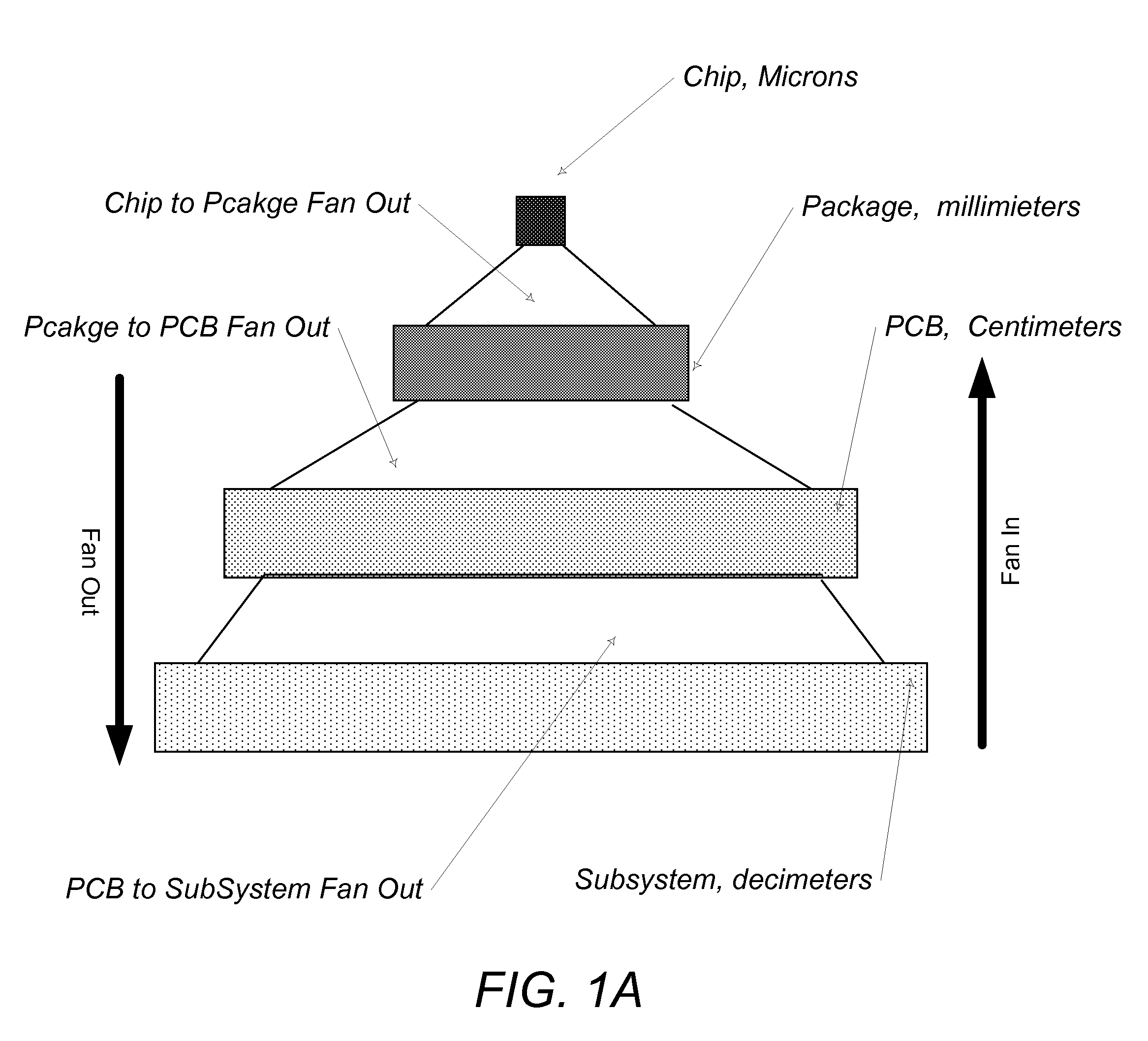
[0029]In summary, the Traditional High Speed Electronic Systems Interconnect experience several bandwidth bottlenecks along the multiplicity of signal paths that limits the information throughput. Here we build upon the cellular interconnect concept of PMTL, the Periodic Micro Transmission Line which was introduced in an earlier patent application, and provide a new type of transmission line VMPL, as the Vertical Micro Transmission Line approach to make all the elements of a high speed interconnect wideband, unified, scalable, and practical for high volume manufacturing. This provides total connectivity improvements from end-to-end of electronic systems that demands higher bandwidth, and increased information throughput, thermal management, and impeccable signal integrity. This is achieved by providing a viable unit cell of high signal integrity TEM transmission line employing the VTCTD, Virtual Thickening of Conductor and Thinning of Dielectrics, of reducing conductor and dielectric losses for high speed connectivity, and using these PMTL-VMTL unit cells as the building blocks of various interconnect components, such as transmission lines, shielded or unshielded, twisted pairs, single ended, differential pairs, cables bundles connectors arrays, 3D via structures, in a logical, systematic, and incremental manner that allows development of proven design manufacturing and testing techniques. This will revolutionize the backplane, motherboard / daughter board interconnect systems, and provide new possibilities for new higher speed topologies and architectures for routers, computers, servers, switches in the communication infrastructures. The technologies introduced here provide solutions for any level of the fan out from chips to systems, in CMOS, or Packages, and PCB's.

Problems solved by technology

One of the greatest impediments to increasing the information throughput in modern networked electronics systems is the limitation of bandwidth of the weakest link in the interconnect chain.
The journey is long, and the possibilities of signal failure are numerous.
Other secondary losses mechanism such as current bunching also effects losses.
But, the coaxial lines are usually manufactured by extrusion and are not very useful in PCB and COMS scales.

Method used


Image

  • Unified scalable high speed interconnects technologies
  • Unified scalable high speed interconnects technologies
  • Unified scalable high speed interconnects technologies

Examples


Embodiment Construction

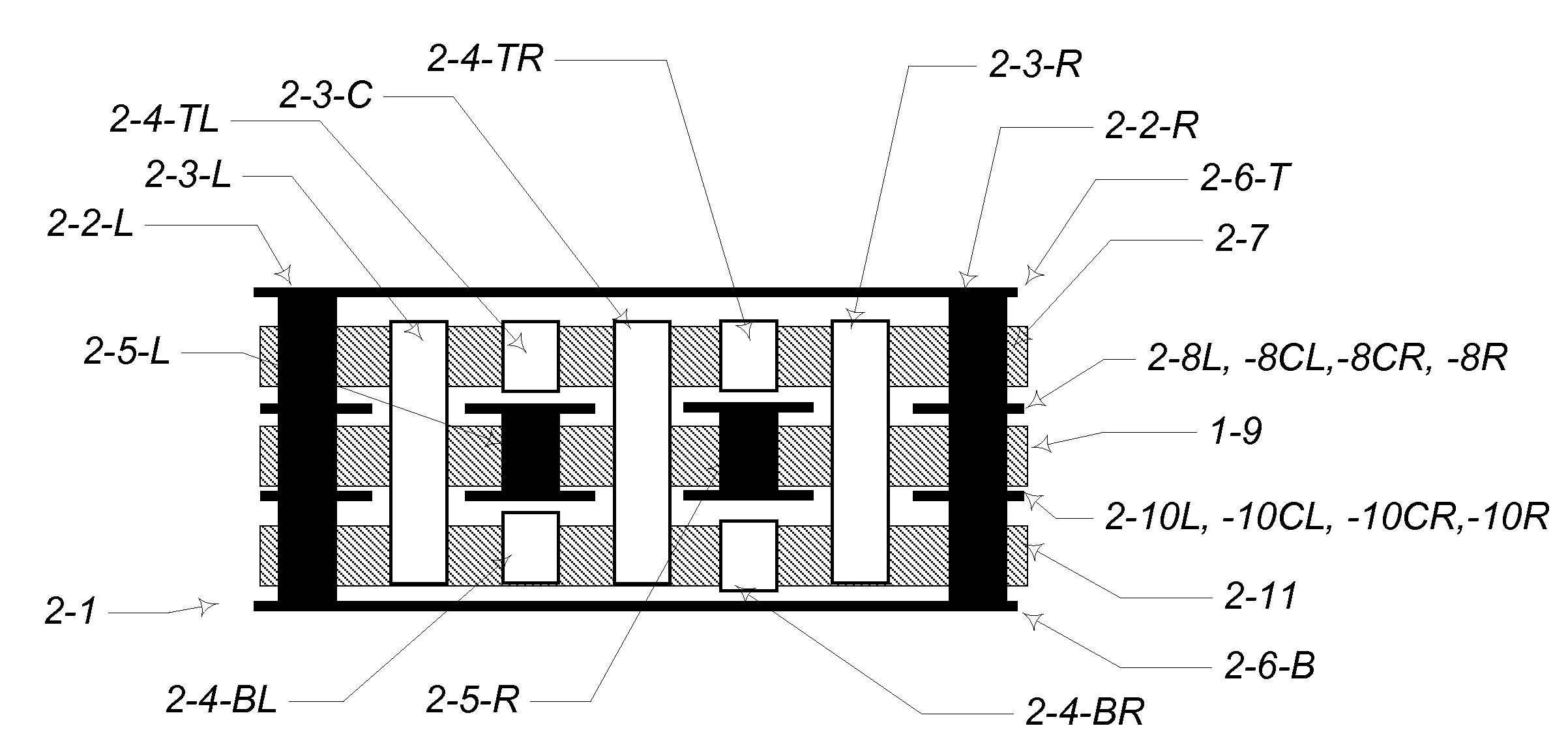
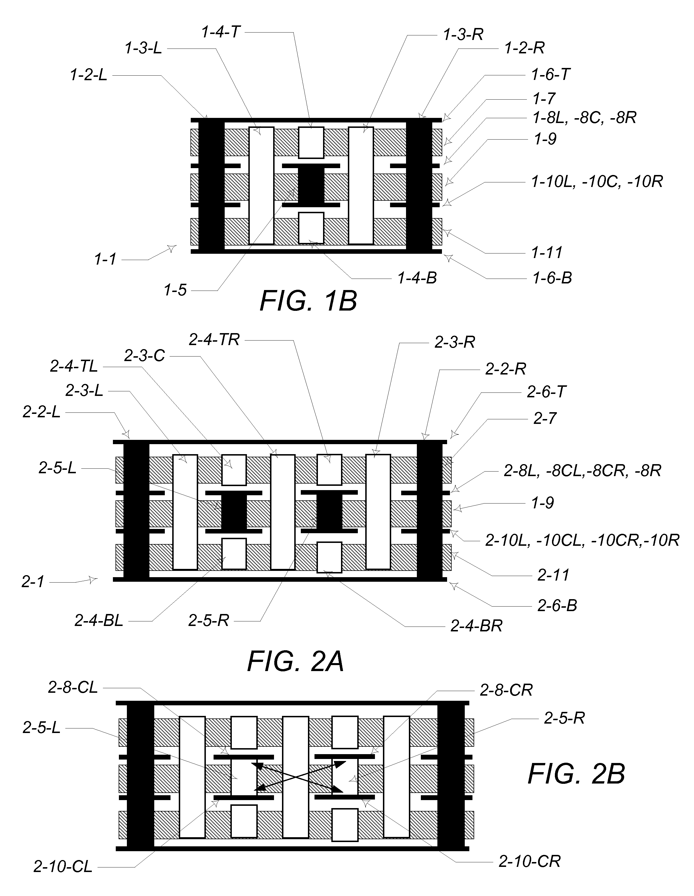
[0146]FIG. 1B shows a cross section of one possible embodiment comprising of four layer PMTL transmission line as was disclosed in Izadian. As is shown, the PMTL can be constructed from strategic use of several dielectric layers, in this case three, designated by 1-7,1-9, and 1-11, and four metal layers, designated by 1-6-T, 1-8, 1-10, and 1-6-B. and a set of Plated Thorough Holes arrays, (PTH) as well as a set of VIA NPTH arrays. (not plated, filled with air or such) strategically arranged. One of the objectives of this arrangement is to emulate the behavior of coaxial transmission line. The PMTL 1-1 of FIG 1B shows a central PTH 1-5 that electrically connects the two central traces 1-8C and 1-10C together thus substantially providing a fat center conductor type assembly. The PMTL also comprise of shield around the center conductor comprised of ground plane 1-6-T on top, and 1-6-B on bottom, which are interconnected through two PTH via stacks of 1-2-L on the left, and 1-2-R on the ...


PUM


Abstract

Traditional High Speed Electronic Systems Interconnect experience several bandwidth bottlenecks along the multiplicity of signal paths that limits the information throughput. Here we build upon the cellular interconnect concept of PMTL, the Periodic Micro Transmission Line which was introduced in an earlier patent application, and provide a new type of transmission line VMPL, as the Vertical Micro Transmission Line approach to make all the elements of a high speed interconnect wideband, unified, scalable, and practical for high volume manufacturing. This provides total connectivity improvements from end-to-end of electronic systems that demands higher bandwidth, and increased information throughput, thermal management, and impeccable signal integrity. The technologies introduced here provide solutions for any level of the fan out from chips to systems, in CMOS, or Packages, and PCB's.

Description

INTRODUCTIONA Review of Prior Art[0001]The objective of carrying signal from one point to another on an electronic system requires a unified approach to the wiring and interconnect. One of the ways that this goal has been achieved between electronic systems separated by large distances has been through twisted pair copper wires, or indeed what has been used since the days of the POTS and Alexander Graham Bell. Although many variations and evolutions has been implemented, the basic technique and the premise stays the same, new innovations merely have tried to package them differently or bundle them as the one cited by U.S. Pat. No. 5,883,334, Newmoyer et al., who discloses a new bundling scheme to try to pack more twisted pairs into the cable. Yet, in another, U.S. Pat. No. 7,449,638 B2, the objective of providing better isolation between quad twisted pairs is addressed, to attempt to limit the intra-interference between the differential twisted pairs of the same cable. Further attem...

Claims


Application Information

Patent Timeline
IPC IPC(8): H05K1/03
CPCH01L23/642H01L23/66H01L2924/01015H01L2924/3025H01L2924/30107H01L2924/3011H01L2224/45147H01L2924/01041H01L2924/01033H01L2924/01024H01L2924/01023H01L24/16H01L24/24H01L24/82H01L25/50H01L2224/02379H01L2224/2402H01L2224/2405H01L2224/24101H01L2224/24145H01L2224/24226H01L2224/48101H01L2224/48227H01L2224/49173H01L2224/82203H01L2924/01013H01L2924/01029H01L2924/01056H01R12/523H05K1/024H05K1/0245H05K1/025H05K1/14H05K1/142H05K2201/044H05K2201/0715H05K2201/09609H05K2201/097H01L2924/01005H01L2924/01006H01L2924/01019H01L2924/00H01L2924/30111H01L2924/00011
Inventor IZADIAN, JAMAL S.
Owner WAYMO LLC
Learn More