Deep ultraviolet light emitting device and method for fabricating same

a technology of ultraviolet light and light-emitting diodes, which is applied in the direction of semiconductor devices, electrical devices, nanotechnology, etc., can solve the problems of crystalline defects, difficult manufacturing, and thermal mismatch between iii-nitride lattice and thermal mismatch, and achieve the effect of reducing thermal impedance and superior performance of the present light-emitting diodes

Active Publication Date: 2010-12-23
NIITEK
View PDF8 Cites 27 Cited by
  • Summary
  • Abstract
  • Description
  • Claims
  • Application Information

AI Technical Summary

Benefits of technology

[0011]The present invention is an ultra-violet light-emitting device and method for fabricating an ultraviolet light emitting device. In a preferred embodiment, the present invention is a deep ultra-violet light-emitting structure (λpeak=200-369 nm) with an AlxInyGa1-x-yN, wherein 0<x≦1, 0≦y≦1, and 0<x+y≦1, quantum-well active region on a template. The template may include a substrate but has two buffer layers, one of which is trenched and the second of which forms a coalesced planar layer over the first. The coalescing involves performing PLOG over deep trenches (height≧0.4 μm in case of AlN), or over shallow or deep trenches if the pillars encompass more than one group III species or a combination of multiple layers. The pillars may consist of a multi-layer stack of III-Nitride based semiconductors including AlN, and a strain-relieving superlattice. In some embodiments additional layers are included in the pillars on top of the superlattice including AlxInyGa1-x-yN (wherein 0<x≦1, 0≦y≦1, and 0<x+y≦1), and additional superlattices with different average composition than the first superlattice. The second buffer layer, of AlN or AlxInyGa1-x-yN (wherein 0<x≦1, 0≦y≦1 and 0&l...

Problems solved by technology

These LEDs are difficult to manufacture for a number of reasons.
For example, defects arise from lattice and thermal mismatch between the group III-Nitride based semiconductor layers and a substrate such as sapphire, silicon carbide, or silicon on which they are constructed.
In addition, impurities and tilt boundaries result in the formation of crystalline defects.
These defects have been shown to reduce the efficiency and lifetime of LEDs and LDs fabricated from these materials.
This method, however, has been shown to be ineffective for the growth of aluminum-containing III-Nitride based semico...

Method used


Image

  • Deep ultraviolet light emitting device and method for fabricating same
  • Deep ultraviolet light emitting device and method for fabricating same
  • Deep ultraviolet light emitting device and method for fabricating same

Examples


Embodiment Construction

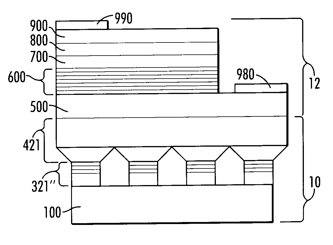
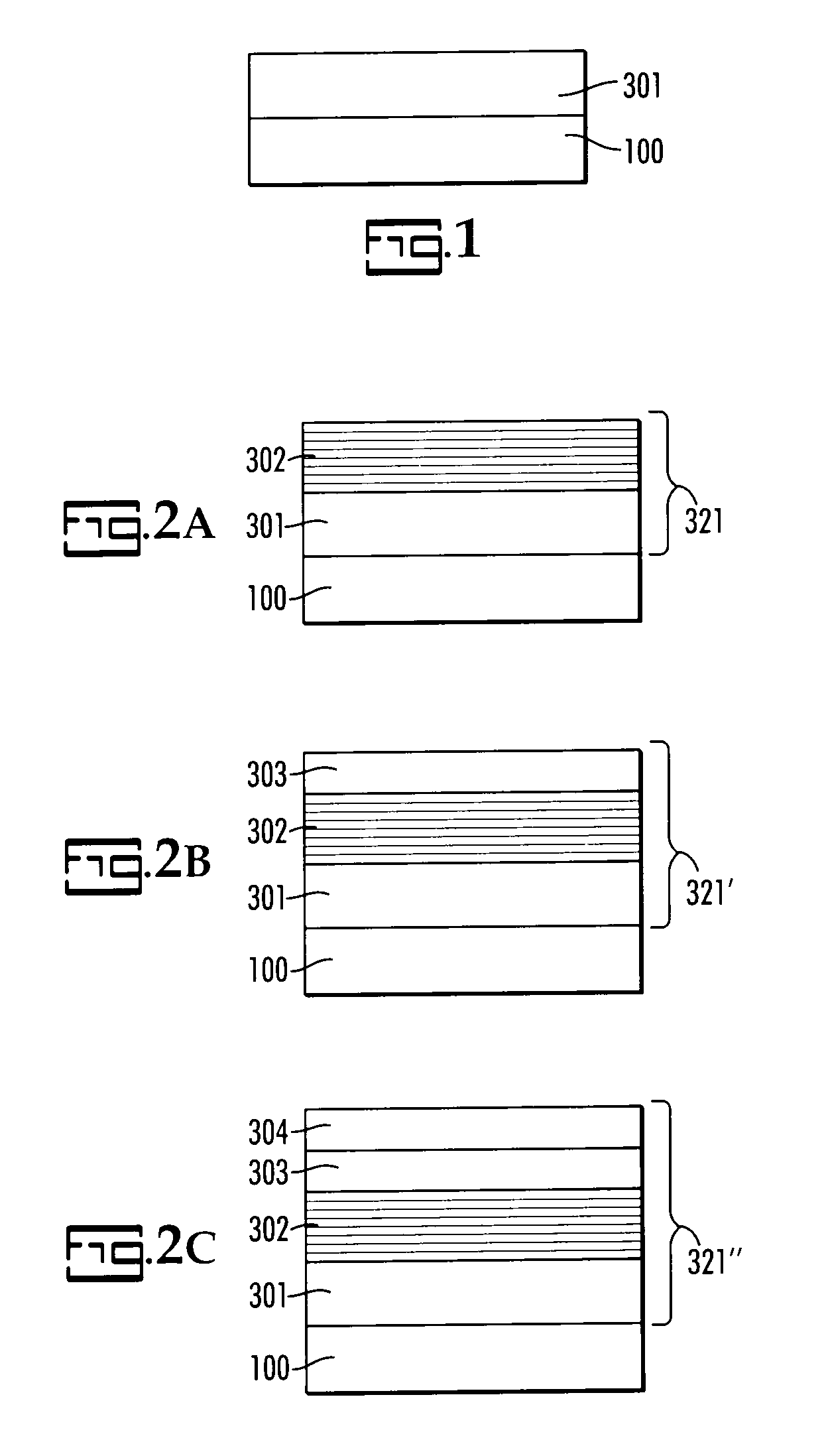
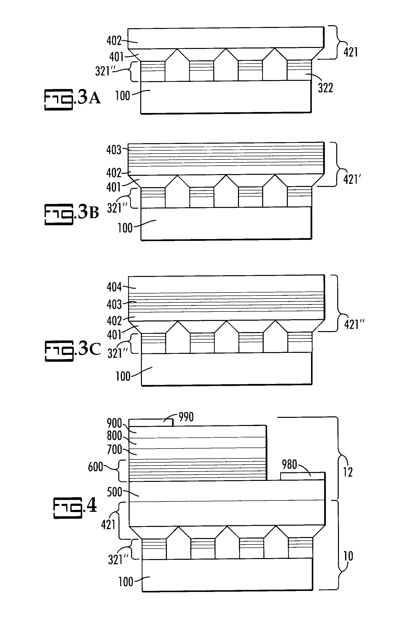
[0027]The present invention is a light-emitting device (LED) and a method for making an LED, particularly one that emits deep ultraviolet light. In particular, it is a template 10 that serves as a platform for an ultraviolet light-emitting structure 12 as shown in FIG. 4. Briefly, template 10 includes a substrate, and a first buffer layer added onto the substrate as the first step in forming the LED wafer. The first buffer layer is then etched to form a pattern of trenches with etch depth greater than or equal to 0.4 μm if the buffer is AlN and the substrate is sapphire, or greater than or equal to 0.1 μm if the first buffer layer consists of one or more AlInGaN layers. After patterning the wafer, a second buffer is applied to the first buffer to cause the patterned wafer to coalesce. Next, the ultraviolet light-emitting structure 12 is applied to template 10. First, a semiconductor layer having a first type of conductivity is applied, followed by several layers forming a quantum-we...


PUM


Abstract

An ultra-violet emitting light-emitting device and method for fabricating an ultraviolet light emitting device (LED) with an AlInGaN multiple-quantum-well active region exhibiting stable cw-powers. The LED includes a template with an ultraviolet light-emitting structure on it. The template includes a first buffer layer on a substrate, then a second buffer layer on the first preferably with a strain-relieving layer in both buffer layers. Next there is a semiconductor layer having a first type of conductivity followed by a layer providing a quantum-well region with an emission spectrum ranging from 190 nm to 369 nm. Another semiconductor layer having a second type of conductivity is applied next. Two metal contacts are applied to this construction, one to the semiconductor layer having the first type of conductivity and the other to the semiconductor layer having the second type of conductivity, to complete the LED.

Description

BACKGROUND OF THE INVENTION[0001]The present invention relates generally to an ultraviolet light-emitting device and method of manufacturing a light-emitting device.[0002]Group III nitride compound semiconductors such as, for instance, gallium nitride (GaN), aluminum nitride (AlN), indium nitride (InN) (hereinafter also referred to as a “Group III-nitride semiconductor” or “III-nitrides”) have been gaining attention as a material for semiconductor devices that emit green, blue or ultraviolet light. A light-emitting diode or a laser diode that emits blue light may be used for displays, for lighting and for high-density optical disk devices. A light-emitting device (which together with the acronym LED, when used herein, will for convenience also refer to both a light-emitting diode and laser diode unless otherwise specified) that emits ultraviolet radiation is expected to find applications in the field of ultraviolet curing, phototherapy, water and air purification, bio-detection, and...

Claims


Application Information

Patent Timeline
IPC IPC(8): H01L33/04H01L33/12H01L33/00H01L33/06H01L33/20
CPCB82Y20/00H01L33/20H01L33/06H01L33/007
Inventor KHAN, ASIF
Owner NIITEK
Why Eureka
Try Eureka