Low noise high thermal conductivity mixed signal package

a high-temperature, mixed-signal technology, applied in the direction of semiconductor devices, semiconductor/solid-state device details, electrical apparatus, etc., can solve the problems of capacitor interaction with parasitic or self-inductance, block damaging electromagnetic radiation transmission, etc., to achieve effective thermal management, high-temperature conductivity materials, and dissipate thermal energy to surrounding air

Active Publication Date: 2011-01-27
RAYTHEON CO
View PDF3 Cites 18 Cited by
  • Summary
  • Abstract
  • Description
  • Claims
  • Application Information

AI Technical Summary

Benefits of technology

The device package includes a stiffening member such as a square ring formed by a continuous side wall comprising a metal e.g. stainless steel, copper, aluminum, or other material having a similar stiffness. The continuous side wall has an outer perimeter forming outside edges of the device package and an inner perimeter enclosing a hollow cavity surrounding the semiconductor die. The continuous side wall has a bottom surface fixedly attached to a top surface of the package substrate by an adhesive layer such that the continuous side wall stiffens the package substrate in order to prevent the semiconductor die from bending or twisting which could lead to die and / or stud bump cracking during thermal expansion or handling. The continuous side wall thickness or height above the package substrate exceeds a height of the semiconductor die.
The device package includes a cover fixedly attached to a top surface of the continuous side wall, e.g. by a layer of adhesive. The cover seals the hollow cavity thereby protecting the semiconductor die from contamination and moisture. In addition, the device package includes a heat spreader disposed between a top surface of the semiconductor die and a bottom surface of the cover and in thermal contact with both. The heat spreader is fabricated from a high thermal conductivity material, such as diamond which generally has a thermal conductivity coefficient of over 900 W / m°K at 20° C. The heat spreader has a cross-sectional area that is larger than the cross-sectional area of the semiconductor die but that still fits inside the hollow cavity. It should be noted that in some applications, the heat spreader can provide effective thermal management even if it does not have a surface area larger than the surface area of the top of the die (e.g., in certain applications, it may be advantageous to have the heat spreader surface area equal to the top surface area. The heat spreader functions to conduct thermal energy away from hot spots in the semiconductor die top surface, and to conduct thermal energy toward the cover. Preferably the cover is formed from copper which generally has a thermal conductivity coefficient of over 400 W / m°K at 20° C. and functions to dissipate thermal energy to surrounding air and to conduct thermal energy from the heat spreader to the continuous side wall. The side wall serves to dissipate thermal energy to the surrounding environment.
The device package includes one or more passive electrical components housed inside the hollow cavity. The passive electrical components may include capacitors and or inductors electrically interconnected to the package substrate or to the semiconductor die by ribbon bonded connections. Other electrical interconnections such as wire bonding or solder bumps may be utilized depending on the selected passive components. Certain passive electrical components function to prevent noise from contaminating the die input / output signals and prevent noise from interfering with proper IC operation. More specifically a plurality of decoupling capacitors may be electrically interconnected with power planes and ground planes of the package substrate to decouple signal transients from power supply inputs to the die. In addition, other passive components, such as high Q inductors may also be interconnected with the package substrate in order to realize other circuit functions, such as adjustable resonant filters.

Problems solved by technology

In addition, the device package may block damaging electromagnetic radiation transmission and facilitate thermal energy dissipation.
Another problem associated with the use of capacitors on PCB's is that capacitors interact with the parasitic or self inductance and resistance inherent in the conductive pathways electrically interconnecting the capacitors with the IC's.
The parasitic inductance and resistance when combined with the capacitance of the decoupling capacitors act like an R-L-C network having resonant frequencies and harmonics capable of injecting additional noise into IC input signals and possibly capable of damaging the IC and / or adversely affect circuit performance.
Recently, as input signal frequencies begin to exceed 1 GHz, the interaction of decoupling capacitors with the parasitic inductance of PCB and package interconnections have become problematic as the R-L-C networks formed by decoupling capacitors on a PCB and package interconnections generate unacceptable signal noise.
Conventional packages are unacceptable for packaging new high speed, high dynamic range (i.e., high signal to noise ratio), high power dissipation, mixed signal die because there are no conventional packages which simultaneously address all 3 of the following requirements: 1) maintain sufficiently low junction temperatures for the high power densities and high overall power dissipation of the new die, 2) contain sufficiently low parasitics in the interconnects within the IC package to achieve a low noise environment and high dynamic range operation in the presence of high speed switching and mixed analog / digital circuitry; and 3) contain adequately short path lengths between the die and critical passive components (such as decoupling capacitors) to minimize parasitics for proper operation of the high speed, high dynamic range circuit.

Method used


Image

  • Low noise high thermal conductivity mixed signal package
  • Low noise high thermal conductivity mixed signal package
  • Low noise high thermal conductivity mixed signal package

Examples


Embodiment Construction

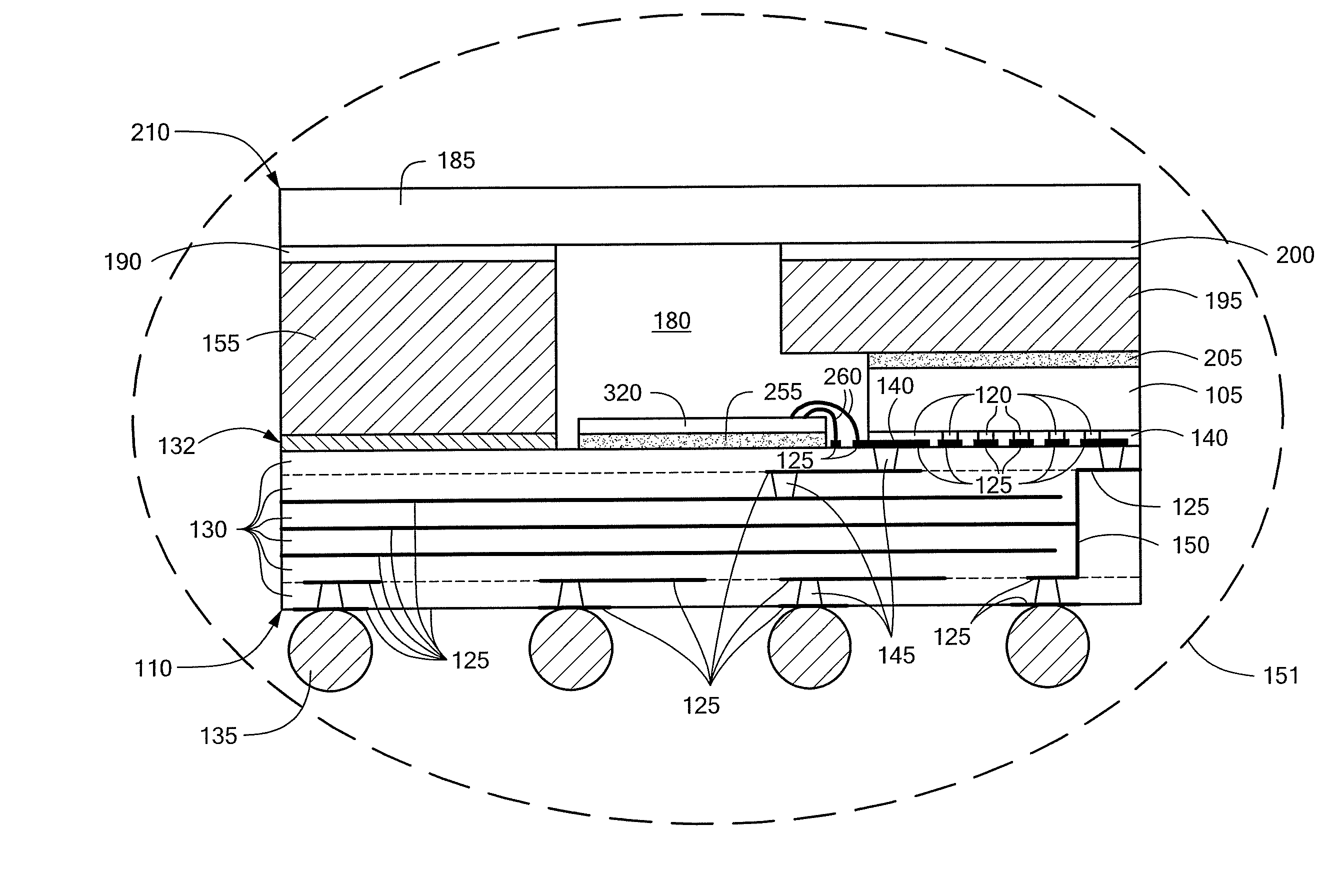
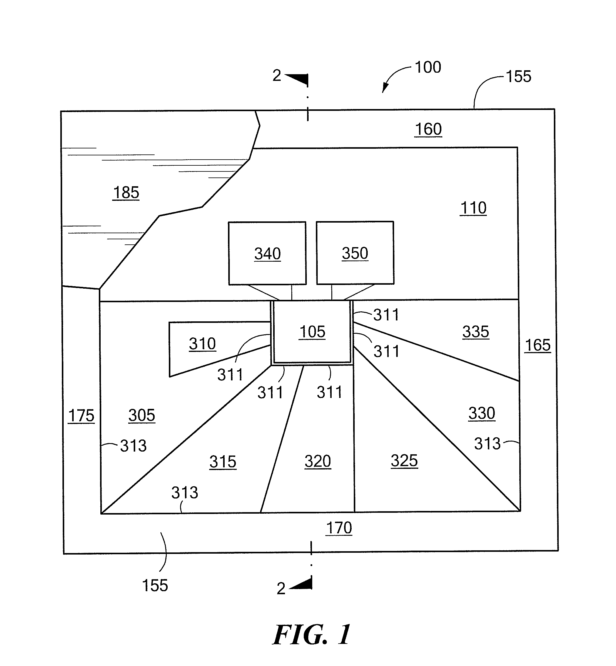
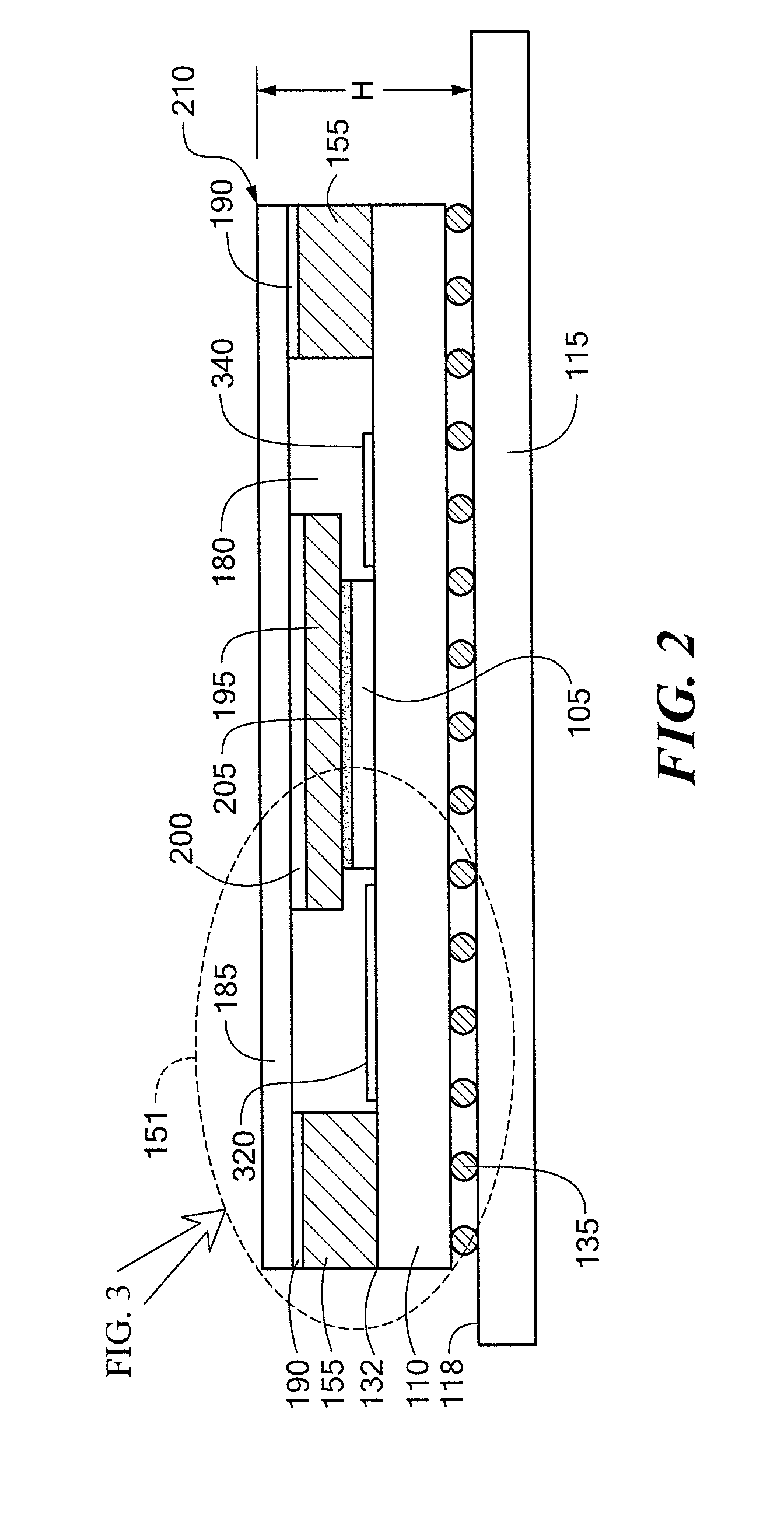
Referring to FIGS. 1 and 2, a microelectronic assembly 100 is shown in top view with its cover 185 partially cut away and heat spreader 195 removed. The microelectronic assembly 100 includes a flip chip semiconductor die 105 packaged in a device package 210 that preferably conforms to Joint Electron Device Engineering Council, (JEDEC) standard microelectronic device package dimensions of 25×25 mm square by approximately 2.9 mm thick, but other package dimensions are usable. The microelectronic assembly 100 includes an array of passive decoupling capacitors 305, 310, 315, 320, 325, 330 and 335 housed inside the device package 210 and electrically interconnected with the semiconductor die 105 using low inductance electrical interconnections.

The microelectronic assembly 100 may further include other components, such as an array of tunable, low profile, high frequency or high Q resonator inductors 340 and 350, electrically interconnected with the semiconductor die 105 as part of resonat...


PUM


Abstract

An improved microelectronic assembly (100) and packaging method includes a device package for housing a semiconductor die or chip, (105), an array of passive electronic components (305-355) operating in cooperation with the flip chip semiconductor die (105) and housed inside the device package to decouple noise from input signals, and a heat spreader (195) disposed between a top surface of the semiconductor die (105) and a package cover (185). The semiconductor die (105) is configured as a flip chip die and the device package includes a package substrate (110) configured as a ball grid array. The improved microelectronic device (100) reduces parasitic inductance in electrical interconnections between the semiconductor die and an electrical system substrate (115) and reduces signal noise in mixed signal high frequency analog to digital converters operating at clock rates above 1 GHz.

Description

BACKGROUND OF THE INVENTION1. Field of the InventionThe present invention relates to an improved microelectronic assembly and packaging method. In particular, the improved microelectronic assembly includes a device package for housing a semiconductor die or chip, an array of passive electronic components operating in cooperation with the semiconductor die and housed inside the device package, and a diamond heat spreader in contact with the semiconductor die to improve the flow of heat.2. Description of the Related ArtElectronics systems assembled on a circuit substrate, e.g. a printed circuit board, (PCB), or the like, generally include one or more microelectronic assemblies and a plurality of passive electronic components surface mounted onto the PCB. The microelectronic assemblies and passive components are electrically interconnected by “PCB interconnections” comprising a series of conductive pathways such as conductive planes or conductive runs or buses on various layers of the ...

Claims


Application Information

Patent Timeline
Patent Type & Authority Applications(United States)
IPC IPC(8): H01L23/34H01L21/60
CPCH01L23/055H01L2924/01019H01L23/16H01L23/3732H01L23/433H01L23/49822H01L23/50H01L23/645H01L2224/16H01L2224/48091H01L2224/48227H01L2224/73204H01L2924/01079H01L2924/14H01L2924/15311H01L2924/16195H01L2924/19041H01L2924/19042H01L2924/19043H01L2924/19105H01L2924/19107H01L2924/30105H01L2924/30107H01L2924/3011H01L23/10H01L2224/73265H01L2224/32225H01L24/48H01L2224/16225H01L2224/45144H01L2924/00014H01L2924/00H01L2924/00012H01L2224/45014H01L24/45H01L24/73H01L2224/73253H01L2924/3511H01L2924/206
Inventor KLING, DENNIS R.CHIGNOLA, BRUCE WILLIAMKATZ, DAVID J.MARCIAL, JORGE M.SCHAPER, LEONARD
Owner RAYTHEON CO
Why Eureka
Try Eureka