Method of manufacturing photoelectric conversion device

a technology of photoelectric conversion and manufacturing method, which is applied in the direction of sustainable manufacturing/processing, final product manufacturing, coatings, etc., can solve the problems of inability to manufacture dense microcrystalline semiconductor films and inability to form dense semiconductor films, and achieve the effect of reducing the proportion of amorphous components in deposited microcrystalline semiconductor films

Inactive Publication Date: 2011-03-03
SEMICON ENERGY LAB CO LTD
View PDF17 Cites 8 Cited by
  • Summary
  • Abstract
  • Description
  • Claims
  • Application Information

AI Technical Summary

Benefits of technology

[0013]It is preferable to increase a reaction pressure and reduce a distance between electrodes in order to grow a crystal of a semiconductor in a gas phase. As the reaction pressure is higher, there is an increase in the probability of collision reaction between radicals generated by glow discharge and between the radical and a reaction gas molecule. By reducing the distance between electrodes, a crystalline deposition precursor is made to reach to a deposition surface of a substrate before being enlarged, and the crystalline deposition precursor becomes a crystal nucleus on the deposition surface. Accordingly, the crystal nucleus is grown, whereby a dense microcrystalline semiconductor film having crystallinity can be formed. Then, the crystalline deposition precursor is generated in a gas phase, whereby a microcrystalline semiconductor film having favorable crystallinity can be formed from the early stage of deposition.
[0014]In addition, it is preferable to add a rare gas to the reactive gas. The rare gas introduced into the reaction chamber together with the reactive gas has the effect of reducing an electron temperature and increasing electron density. Accordingly, the amount of the generated radicals is increased, a film formation rate is improved, crystallinity of a microcrystalline semiconductor film is improved, and thus the microcrystalline semiconductor film is densified. In order to obtain such an effect, it is necessary to excite the rare gas so as to be placed in a metastable state and therefore it is necessary to generate excited species of the rare gas or apply an electric field sufficient for ionization of the rare gas. For example, when argon is added as the rare gas in addition to a silane gas and a hydrogen gas which are reactive gases, a hydrogen radical increases in number and crystallinity of a microcrystalline semiconductor film can be improved.
[0018]In the above structure, the electron temperature of the high-density plasma region is reduced and electron density in the high-density plasma region is increased by adding a rare gas to the reactive gas, so that the crystallinity of the microcrystalline semiconductor film can be improved.
[0022]As described above, a proportion of amorphous components included in a deposited microcrystalline semiconductor film can be reduced; thus, a dense microcrystalline semiconductor film can be manufactured.

Problems solved by technology

However, a conventional plasma CVD apparatus has a structural defect in which an electric field is locally concentrated and therefore has not been able to manufacture a dense microcrystalline semiconductor film.
Accordingly, a dense semiconductor film has not been able to be formed.

Method used


Image

  • Method of manufacturing photoelectric conversion device
  • Method of manufacturing photoelectric conversion device
  • Method of manufacturing photoelectric conversion device

Examples


embodiment 1

[0044]In this embodiment, a method for manufacturing a microcrystalline semiconductor film having high crystallinity is described with reference to FIGS. 1A and 1B, FIG. 2, FIGS. 3A and 3B, and FIG. 4.

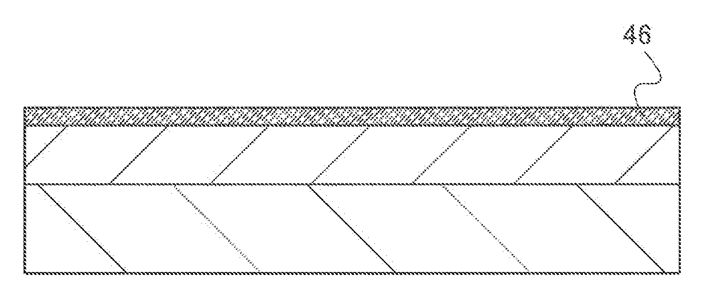
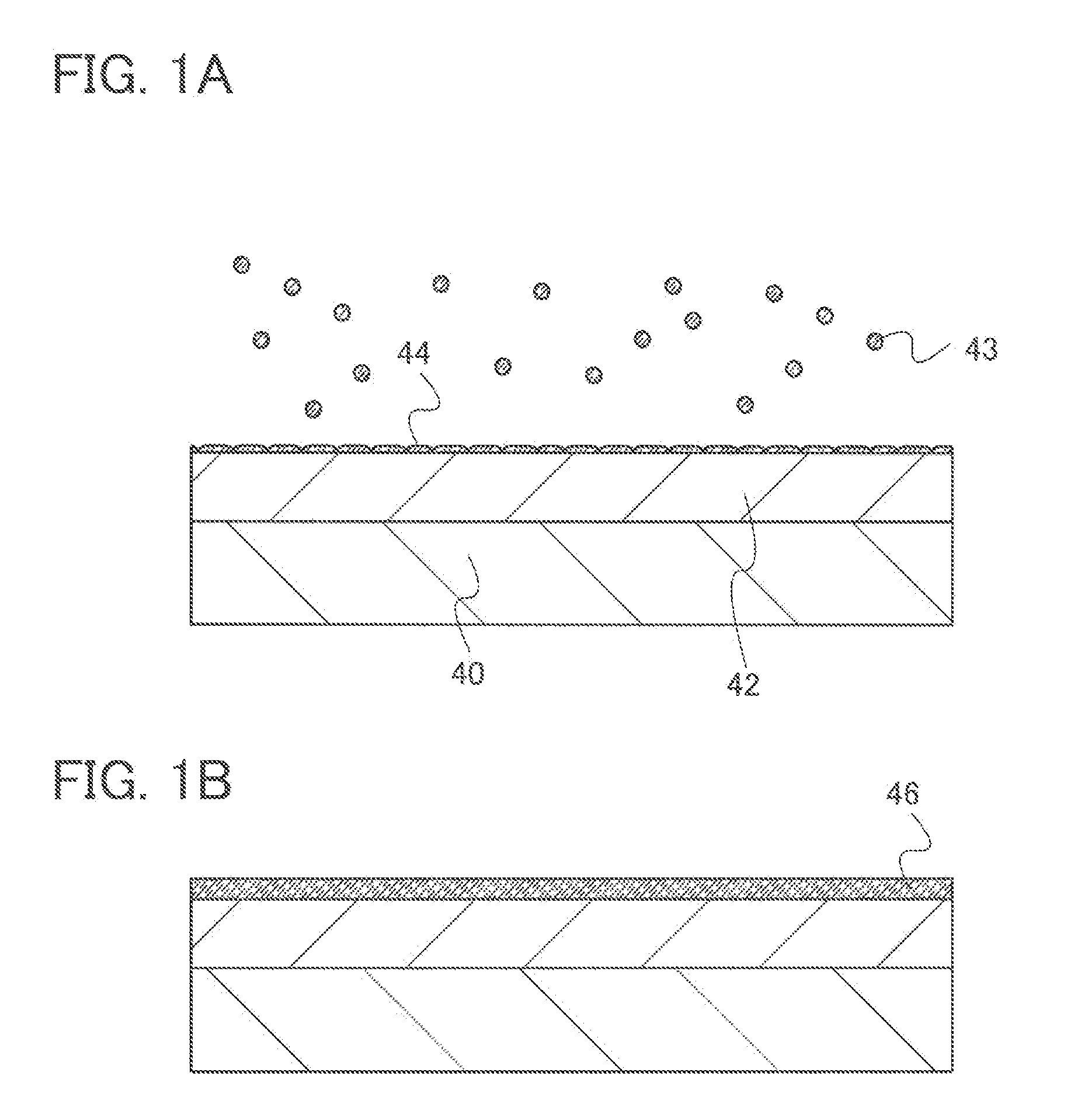
[0045]As illustrated in FIG. 1A, in a method for manufacturing a microcrystalline semiconductor film shown in this embodiment, deposition precursors 43 are formed in a gas phase, the deposition precursors 43 are deposited over a base film 42 which is formed over a substrate 40, and crystal nuclei 44 are formed. Next, as illustrated in FIG. 1B, a microcrystalline semiconductor film is formed over the crystal nuclei 44, whereby crystals are grown using the crystal nuclei 44 as nuclei so that a microcrystalline semiconductor film 46 can be formed.

[0046]The deposition precursor 43 is formed through reaction of electrons and a source gas in plasma. The pressure in a film formation chamber can be higher than a film formation pressure of 300 Pa for a conventional microcrystalline semiconducto...

embodiment 2

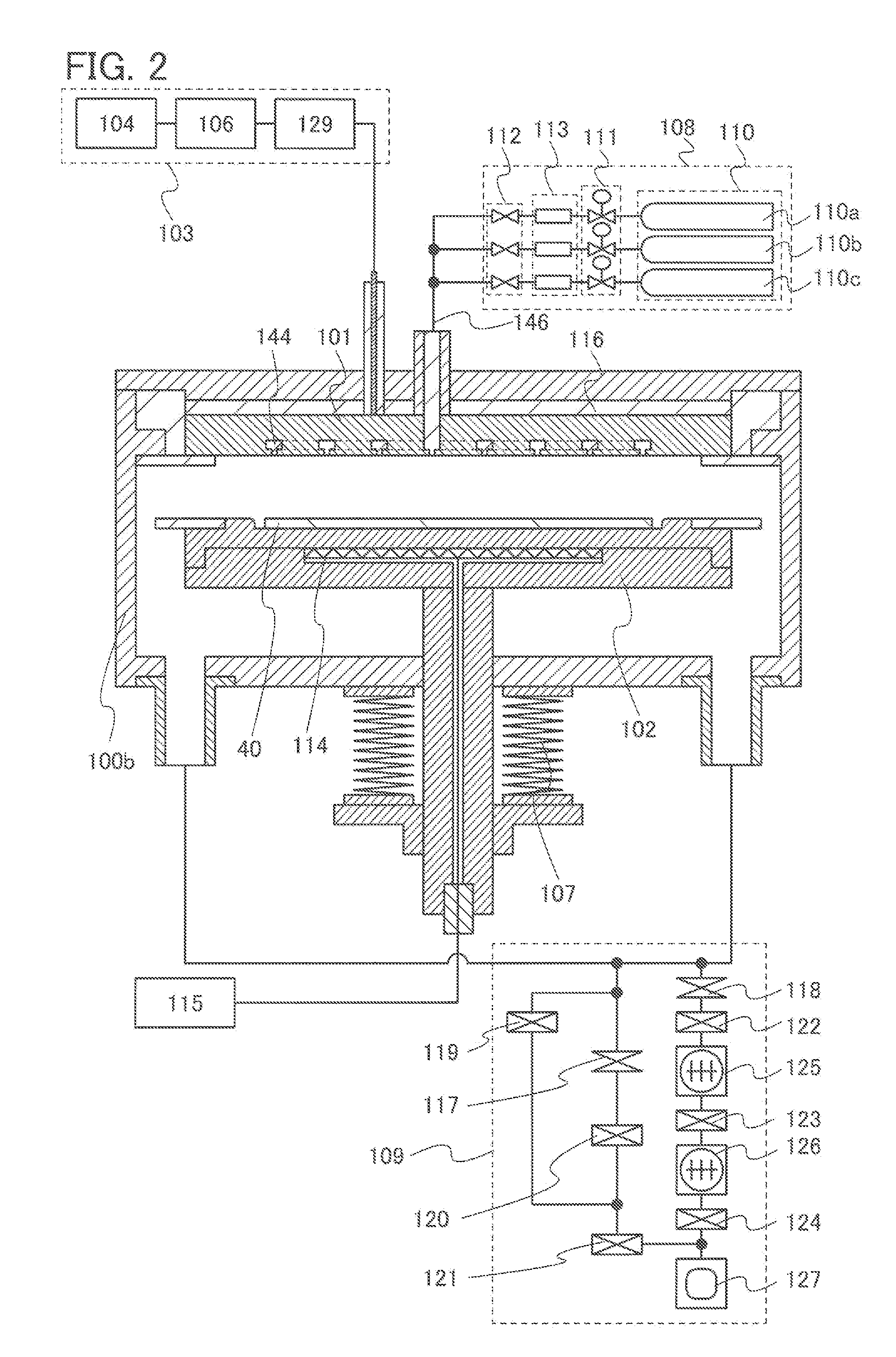
[0081]In this embodiment, a structure applicable to the first electrode of the plasma CVD apparatus shown in Embodiment 1 is described with reference to FIG. 5, FIGS. 6A and 6B, FIGS. 7A and 7B, FIGS. 8A and 8B, FIGS. 9A and 9B, and FIGS. 10A to 10D.

[0082]In a structure of the reaction chamber of the plasma CVD apparatus illustrated in FIG. 5, the first electrode 101 is an electrode that is projected and depressed by having projected portions 141 and depressed portions 143 arranged regularly, preferably at regular intervals. In other words, the projected portions 141 formed using projected structure bodies are arranged regularly, preferably at regular intervals. The hollow portions 144 connected to the gas supply unit 108 are provided in the depressed portions 143 of the first electrode 101. In other words, the depressed portions 143 form a common plane where gas supply ports are provided. Here, the region having the gas supply port near a surface of the second electrode 102 is rega...

embodiment 3

[0099]In this embodiment, a structure applicable to the first electrode of the plasma CVD apparatus shown in Embodiment 1 is described with reference to FIGS. 9A and 9B. FIG. 9A is a plan view of the first electrode 101 seen from the second electrode 102 side. FIG. 9B is a cross-sectional view taken along A-B in FIG. 9A. Note that in FIG. 9A, regions which are depressed (that is, depressed portions) are shown in fine hatching for clear illustration of the state of the projection and depression.

[0100]As illustrated in FIGS. 9A and 9B, gas supply ports of hollow portions 142 formed in the projected portions 141 are provided regularly, preferably at regular intervals. Further, as illustrated in FIG. 9B, the gas supply ports of the hollow portions 142 are provided in the projected portions 141. The plurality of projected portions 141 are separated from one another, and the depressed portions 143 form a continuous plane (common plane). Here, the projected portions 141 each have the shape...


PUM

PropertyMeasurementUnit
pressureaaaaaaaaaa
distanceaaaaaaaaaa
frequencyaaaaaaaaaa

Abstract

Provided is a technique for manufacturing a photoelectric conversion element using a dense crystalline semiconductor film without a cavity between crystal grains. A method of manufacturing a photoelectric conversion device having a first electrode, a unit cell, and a second electrode over a substrate includes the steps of: forming a plasma region between a first electrode and a second electrode by supplying high-frequency power of 60 MHz or less to the first electrode under a condition where a pressure of a reactive gas in a chamber of a plasma CVD apparatus is set to from 450 Pa to 13332 Pa, and a distance between the first electrode and the second electrode of the plasma CVD apparatus is set to from 1 mm to 20 mm, preferably, 4 mm to 16 mm; forming deposition precursors including a crystalline semiconductor in a gas phase including the plasma region; forming a crystal nucleus having a grain size of from 5 nm to 15 nm by depositing the deposition precursors; and forming a semiconductor film having a first conductivity type, a semiconductor film effective in photoelectric conversion, or a semiconductor film having a first conductivity type in the unit cell, by growing a crystal from the crystal nucleus.

Description

BACKGROUND OF THE INVENTION[0001]1. Field of the Invention[0002]An embodiment of the present invention relates to a method of manufacturing a photoelectric conversion device including a crystalline semiconductor film using a vapor deposition method.[0003]2. Description of the Related Art[0004]In a technical field of thin film transistors, a plasma chemical vapor deposition (plasma CVD) method which is used for manufacture of a semiconductor film is employed, and various improvements have been attempted to manufacture products with higher yields.[0005]For example, an electrode structure of a plasma CVD apparatus is disclosed where an electrode for generating plasma in a reaction chamber is provided with cylindrical recessed portions and the cylindrical recessed portions are connected to each other through a groove which is narrower than the diameter of the cylindrical recessed portion (see Patent Document 1).[0006]In addition, disclosed is a gas diffuser plate (a so-called shower pla...

Claims


Application Information

Patent Timeline
Patent Type & Authority Applications(United States)
IPC IPC(8): H01L31/18
CPCC23C16/45557C23C16/45565C23C16/5096H01L21/02532H01L31/046H01L31/03921H01L31/077H01L31/1824Y02E10/545H01L21/0262H01L31/0463H01L31/0465Y02E10/547Y02P70/50
Inventor HIURA, YOSHIKAZUKATAISHI, RIHOYAMAZAKI, SHUNPEI
Owner SEMICON ENERGY LAB CO LTD
Why Eureka
Try Eureka