
Base material for growing single crystal diamond and method for producing single crystal diamond substrate

Inactive Publication Date: 2011-04-14
SHIN ETSU CHEM IND CO LTD
View PDF8 Cites 17 Cited by
  • Summary
  • Abstract
  • Description
  • Claims
  • Application Information

AI Technical Summary

Benefits of technology

The present invention was accomplished in view of the aforementioned problems, and it is an object of the present invention to provide a base material for growing a single crystal diamond and a method for producing a single crystal diamond substrate which can grow the single crystal diamond having a large area and good crystallinity and produce a high quality single crystal diamond substrate at low cost.
As described above, the base material for growing a single crystal diamond and the method for producing a single crystal diamond substrate according to the present invention can grow the single crystal diamond having a large area and high crystallinity at low cost and produce a high quality single crystal diamond substrate at good productivity.

Problems solved by technology

However, it is difficult to grow in size, while the HPHT single crystal diamond having high crystallinity can be obtained.
In addition, a price of the diamond becomes extremely high when its size becomes big and consequently, it is difficult to put it into practical use as the substrate for the devices.
However, in this method, since the base material and the single crystal diamond grown are composed of the same material, it is difficult to separate these, and there are cost problems that the base material needs implanting ions in advance, a lengthy wet etching separation treatment after the growth and the like.
There is also another problem that crystallinity of the single crystal diamond to be obtained deteriorates to a certain degree due to the ion implantation of the base material.
However, in this method, there is a problem that the base material and the single crystal diamond grown are finely broken due to stress generated between the single crystal MgO substrate and the single crystal diamond grown via the single crystal Ir film (sum of internal stress and heat stress).
Moreover, the crystallinity of the single crystal diamond to be obtained does not achieve a satisfactory level since crystallinity of an available single crystal MgO that is the seed base material is not sufficient.

Method used


Image

  • Base material for growing single crystal diamond and method for producing single crystal diamond substrate
  • Base material for growing single crystal diamond and method for producing single crystal diamond substrate
  • Base material for growing single crystal diamond and method for producing single crystal diamond substrate

Examples


example 1

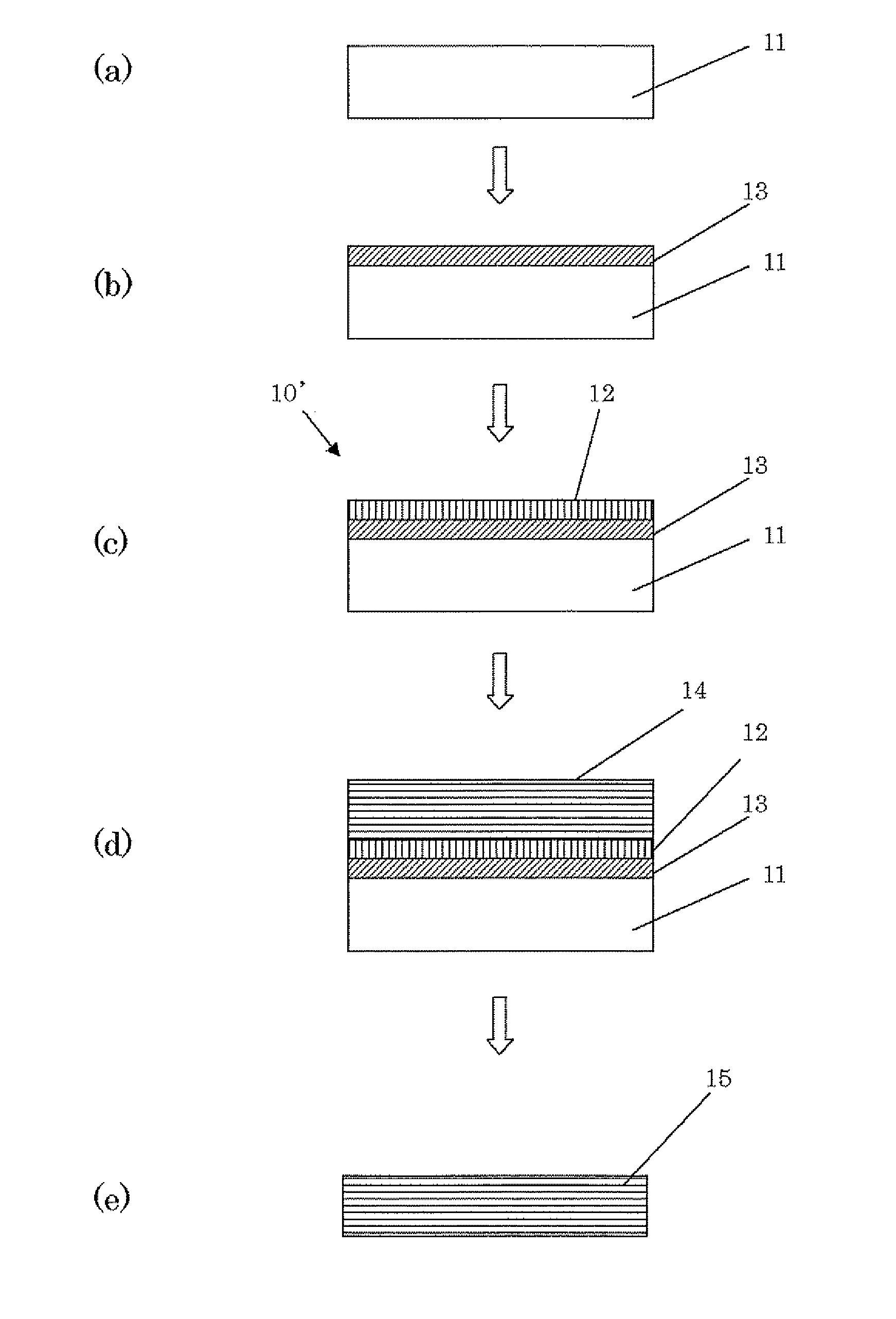
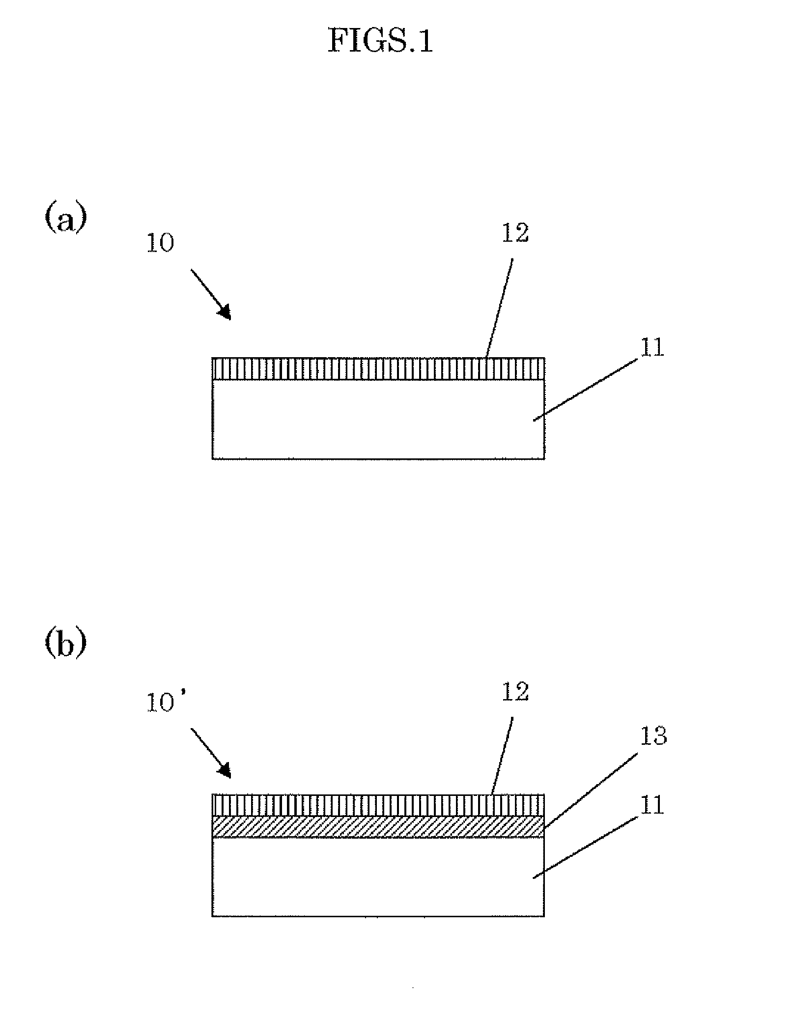
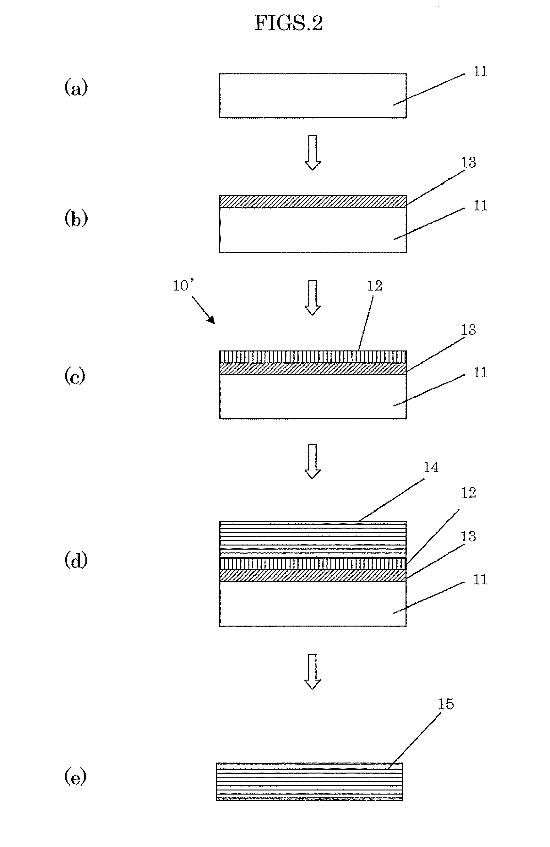
As the seed base material, there was prepared a double-side-polished single crystal β-SiC substrate having a diameter of 20.0 mm, a thickness of 0.25 mm and an orientation (100). The MgO film having a thickness of 0.1 μm was epitaxially grown, by the electron beam evaporation method, on the side of the seed base material where the single crystal diamond was to be grown in a vacuum under the conditions of a substrate temperature of 800° C.

Next, the iridium (Ir) film was heteroepitaxially grown on the single crystal MgO film. The film-forming was completed by performing the sputtering with the R. F. magnetron sputtering method in which an target was Ir under the conditions of an Ar gas of 8 Pa (6×10⁻² Torr) and a substrate temperature of 700° C., until a thickness of the single crystal Ir film became 1.5 μm.

For the sake of electrical continuity in the bias treatment and the direct-current plasma CVD, the Ir film having a thickness of 1.5 μm was also grown on a back surface under the s...

example 2

Except for heteroepitaxially growing the It film directly without forming the MgO film on the β-SiC substrate that was the seed base material, the single crystal diamond was heteroepitaxially grown as with Example 1.

A product taken out from the bell jar was a laminated structure of the diamond / Ir / SiC without the break. In this case, since the product was composed of only high chemical resistance materials and was not able to separate by the wet etching with hot mixed acid, it was cut with laser at the vicinity of the interfaces between the diamond and the Ir to get self-standing structure of the single crystal diamond (the single crystal diamond substrate). The surface was also subjected to a final polishing so that it was finished so as to have surface roughness of a usable level for device application.

It was confirmed that the obtained single crystal diamond substrate had sufficient crystallinity as a result of evaluation by raman spectroscopy, XRD rocking curve, X-sectional TEM a...


PUM


Abstract

The present invention is a base material for growing a single crystal diamond comprising: at least a single crystal SiC substrate; and an iridium film or a rhodium film heteroepitaxially grown on a side of the single crystal SiC substrate where the single crystal diamond is to be grown. As a result, there is provided a base material for growing a single crystal diamond and a method for producing a single crystal diamond substrate which can grow the single crystal diamond having a large area and good crystallinity and produce a high quality single crystal diamond substrate at low cost.

Description

BACKGROUND OF THE INVENTION1. Field of the InventionThe present invention relates to a base material for growing a single crystal diamond and a method for producing a single crystal diamond substrate.2. Description of the Related ArtDiamond has a wide band gap of 5.47 eV and a very high dielectric breakdown electric field intensity of 10 MV / cm, and it has the highest thermal conductivity in materials. Therefore, if this is used for an electronic device, the device is advantageous as a high output power device.Furthermore, the diamond has a high drift mobility and is the most advantageous as a high speed power device among semiconductors in comparison of Johnson performance index.The diamond is thus said to be the ultimate semiconductor suitable for high frequency / high power electronic devices, and accordingly studies of various kinds of electronic devices using a single crystal diamond as a substrate have progressed.Now, a single crystal diamond for producing a diamond semiconductor...

Claims


Application Information

Patent Timeline
IPC IPC(8): H01L29/16H01L21/04
CPCC30B25/06C30B25/18C30B25/183C30B29/04C30B29/02C30B29/16C30B29/36C30B33/08
Inventor NOGUCHI, HITOSHI
Owner SHIN ETSU CHEM IND CO LTD
Learn More