Thin-film photoelectric converter and fabrication method therefor

Inactive Publication Date: 2011-06-23
KANEKA CORP
View PDF5 Cites 11 Cited by
  • Summary
  • Abstract
  • Description
  • Claims
  • Application Information

AI Technical Summary

Benefits of technology

[0030]By setting the absorption coefficient of an infrared-absorption peak at 935±5 cm−1 of the crystalline germanium semiconductor of a photoelectric conversion layer to less than 6000 cm−1, it is considered that formation of germanium hydride or germanium oxide in a polymer or cluster state can be suppressed so that dense crystalline germanium is formed; thus, light having long wavelengths exceeding 1100 nm can be utilized by the thin-film photoelectric converter, and the FF is enhanced so that the characteristics of the thin-film photoelectric converter are improved.
[0031]Furthermore, by setting a refractive index relative to a wavelength of 600 nm of the crystalline germanium semiconductor to 4.0 or more, preferably, to 4.7 or more, more preferably, to 4.9 or more, dense crystalline germanium is formed; thus, light having long wavelengths exceeding 1100 nm can be utilized by the thin-film photoelectric converter, and the FF is enhanced so that the characteristics of the thin-film photoelectric converter are improved.

Problems solved by technology

However, it has been confirmed that in comparison with a-Si, the a-SiGe layer, which is an alloy layer, has a higher defect density with its semiconductor characteristics being deteriorated, and also has an increase in defect density due to irradiation with light.
For this reason, the triple-junction stacked-type thin-film photoelectric converter in which a-SiGe is used for the photoelectric conversion layer of the middle cell or the bottom cell is insufficient in improving the efficiency, in comparison with the double-junction thin-film photoelectric converter.
Moreover, since the photodegradation of a-SiGe is serious, a problem arises that, although the triple-junction stacked-type thin-film photoelectric converter is used, it is not possible to sufficiently suppress the photodegradation.
Therefore, the wavelength to be utilized on the long wavelength side is the same as the wavelength of a double-junction thin-film photoelectric converter, which fails to provide improvements, resulting in a problem that the improvement of the conversion efficiency of the triple-junction thin-film photoelectric converter is insufficient.

Method used


Image

  • Thin-film photoelectric converter and fabrication method therefor
  • Thin-film photoelectric converter and fabrication method therefor
  • Thin-film photoelectric converter and fabrication method therefor

Examples


example 1

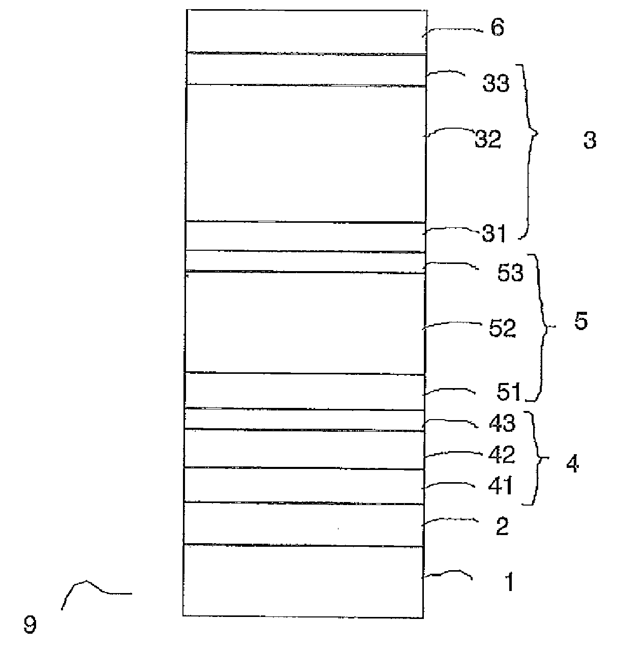
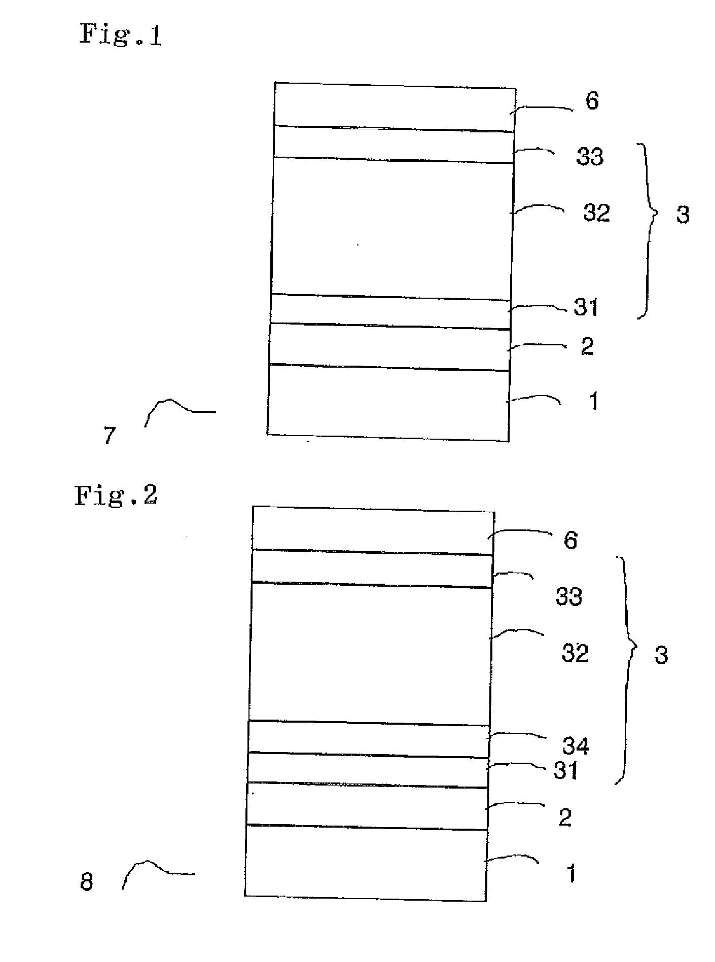
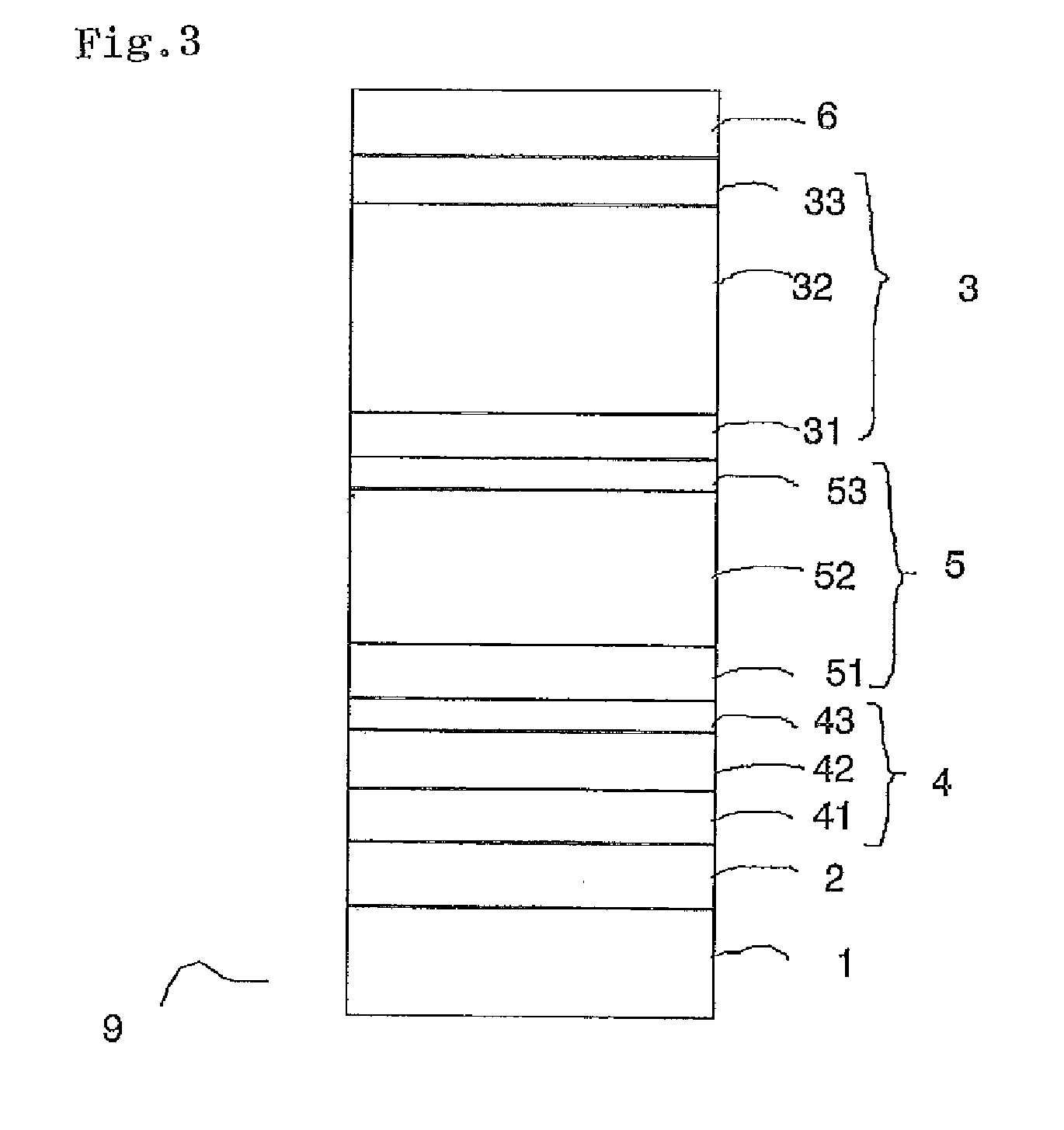
[0121]A single-junction thin-film photoelectric converter 7 having a structure shown in FIG. 1 was manufactured as Example 1. As a transparent substrate 1, a glass substrate having a thickness of 0.7 mm was used. On the transparent substrate 1, an SnO2 film having an average thickness of 700 nm, with fine pyramid-shaped surface irregularities contained therein, was formed by a thermal CVD method. Further, a ZnO film doped with Al was formed thereon with a thickness of 20 nm by using a sputtering method so that a transparent electrode layer 2 in which SnO2 and ZnO were stacked was formed. The resulting transparent electrode layer 2 had a sheet resistivity of about 9 Ω / square. The haze ratio measured by using a illuminant C was 12%, and an average level difference d of the surface irregularities was about 100 nm. The haze ratio was measured based upon JIS K7136.

[0122]On this transparent electrode layer 2, a crystalline germanium photoelectric conversion unit 3 was manufactured by usin...

example 2

[0133]As Example 2, a single-junction thin-film photoelectric converter similar to that of Example 1 was manufactured. The converter of Example 2 was manufactured in the same manner as in Example 1, except that the crystalline germanium photoelectric conversion layer of FIG. 1 was formed at 400° C.

[0134]An absorption coefficient at a wavelength of 1300 nm, measured in the same manner as in Example 1, was 1620 cm−1, which exhibited a high absorption coefficient relative to light with long wavelengths. An X-ray diffraction spectrum is shown in FIG. 4. A particularly strong peak in (220) orientation is observed so that its crystallization state was confirmed. The peak intensity ratio of (220) / (111) was 91. The crystal grain size found by a half-value width of the (220) peak was 51 nm. A Raman scattering spectrum is shown in FIG. 5. A sharp peak in a TO mode of a crystal Ge—Ge bond was observed near 300 cm−1, thereby indicating a crystallization.

[0135]As shown in FIG. 8, although the in...

examples 1 and 2

Summary of Examples 1 and 2 and Comparative Example 1

[0137]In Example 2, no absorption peaks were observed at infrared rays of 935 cm−1 and 960 cm−1, the quantum efficiency of long wavelengths had a high value exceeding 10%, and the Jsc had a high value exceeding 30 mA / cm2. It is considered that the reason why the Eff was slightly lower than that of Example 1 is because diffusion of impurities occurred between the p-type layer and the crystalline germanium layer due to a high film-deposition temperature caused by the reduction in Voc and FF. In each of Examples 1 and 2 and Comparative Example 1, the Raman scattering spectrum of the crystalline germanium layer indicated a crystallization, and no remarkable difference was confirmed. In contrast, with respect to the infrared-absorption peaks at 935 cm−1 and 960 cm−1 and (220) / (111) peak intensity ratio of the X-ray diffraction, remarkable differences were observed; thus, it was found that upon determining the quality of the crystalline...


PUM


Abstract

A conventional thin-film photoelectric converter using amorphous germanium or crystalline silicon as a photoelectric conversion layer is problematic in that light having a long wavelength of 1100 nm or more cannot be used for photoelectric conversion, and is inefficient. The problem is solved by a thin-film photoelectric converter including one or more photoelectric conversion units each having a photoelectric conversion layer sandwiched between a p-type semiconductor layer and an n-type semiconductor layer, wherein the photoelectric conversion layer of at least one photoelectric conversion unit includes an intrinsic or weak n-type crystalline germanium semiconductor, and the absorption coefficient of infrared-absorption peak at wave number of 935±5 cm−1 of the crystalline germanium semiconductor is less than 6000 cm−1. The problem is also solved by a thin-film photoelectric converter having an crystalline germanium semiconductor whose absorption coefficient of infrared-absorption peak at wave number of 960±5 cm−1 of the is less than 3500 cm−1.

Description

TECHNICAL FIELD[0001]The invention relates to improvements in a thin-film photoelectric converter, and more specifically, relates to improvements of utility efficiency of light having long wavelengths by utilizing a crystalline germanium semiconductor. In the present specification, the terms “crystalline” and “microcrystalline” are also applied to a state in which an amorphous structure is partially included, as has been used in the relevant technical field.BACKGROUND ART[0002]In recent years, public attention has been focused on a photoelectric converter that converts light to electricity by utilizing a photoelectric effect inside a semiconductor, and development of the device has been vigorously carried out. Among these developments, a silicon-based thin-film photoelectric converter has been promising as a device that can achieve low costs, because it can be formed on a glass substrate or a stainless substrate with a large area, at low temperatures.[0003]This silicon-based thin-fi...

Claims


Application Information

Patent Timeline
IPC IPC(8): H01L31/0232H01L31/0368H01L31/18
CPCH01L31/028H01L31/075Y02E10/547H01L31/1804Y02E10/548H01L31/076Y02P70/50
Inventor SASAKI, TOSHIAKIKADOTA, NAOKI
Owner KANEKA CORP
Why Eureka
Try Eureka