Single-crystal silicon carbide and single-crystal silicon carbide wafer

Active Publication Date: 2011-08-25
SHOWA DENKO KK
View PDF10 Cites 39 Cited by
  • Summary
  • Abstract
  • Description
  • Claims
  • Application Information

AI Technical Summary

Benefits of technology

[0042]The single-crystal SiC of the present invention is low in defects, so that a wafer made f

Problems solved by technology

The method set out in Patent Literature 1 does not enable total avoidance of defect occurrence at the start of crystal growth, i.e., at the interface between the seed crystal and the grown crystal.
Even though the high-quality final seed crystal is used in the final Nth growth, the occurrence of defects at the start of the growth makes it impossible to produce crystal of a quality higher than that of the seed crystal.
Even with the met

Method used


Image

  • Single-crystal silicon carbide and single-crystal silicon carbide wafer
  • Single-crystal silicon carbide and single-crystal silicon carbide wafer

Examples


example 1

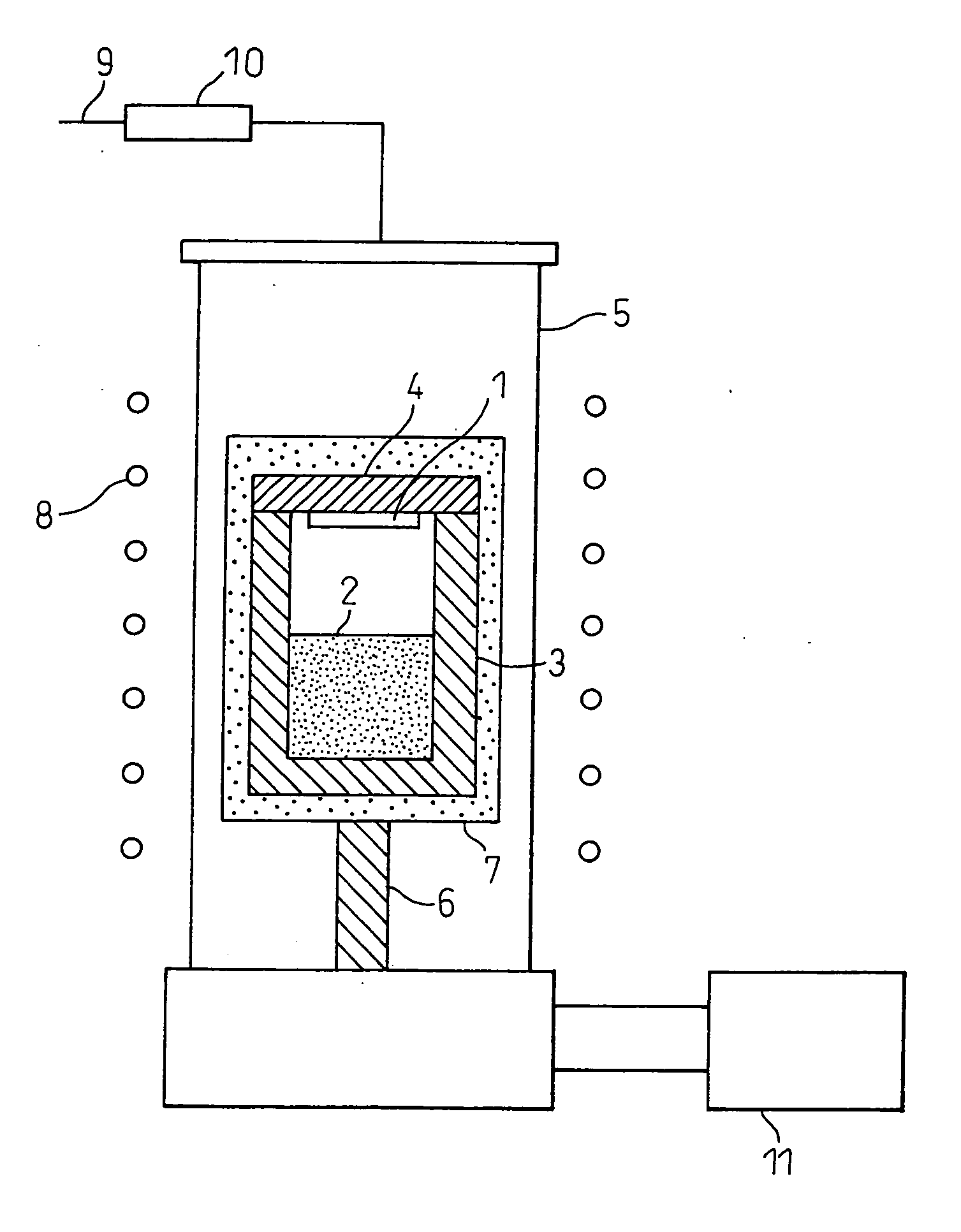
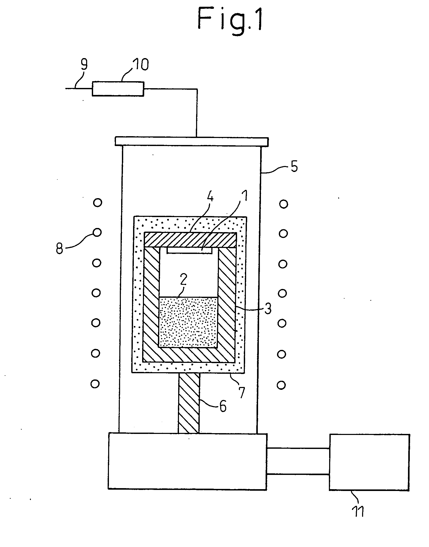
[0057]First, a single-crystal SiC ingot was prepared to obtain a seed crystal for conducting the crystal growth of Example 1.

[0058]A 79 mm diameter single-crystal SiC ingot was produced by a growth process using the aforesaid single crystal growing apparatus under conditions such that the nitrogen concentration in the grown crystal was 2.2×1019 cm−3 in the region 1 mm and greater away from the interface with the seed crystal. In order to obtain the desired value of the grown crystal nitrogen concentration, the partial pressure of the nitrogen gas in the atmosphere was controlled to 100 Pa from the time that the grown crystal was estimated to have reached 1 mm up to the end of growth, and the value of the partial pressure of the nitrogen gas at the start of growth was determined with consideration to the nitrogen concentration and the like of the seed crystal. Next, the so-obtained single-crystal SiC ingot to be used for seed crystals was machined to fabricate a number of 77 mm diame...

example 2

[0064]In order to prepare a seed crystal for conducting the crystal growth of Example 2 by a growth process using the aforesaid single crystal growing apparatus, a 103 mm diameter single-crystal SIC ingot was produced wherein the nitrogen concentration in the grown crystal was 5.1×1019 cm−3 in the region 2 mm and greater from the interface with the seed crystal. In this case, the nitrogen gas partial pressure was controlled to 230 Pa except at the start of growth. The ingot was machined to fabricate a number of 101 mm diameter wafers of an off-angle of 8° from the {0001} plane. Both sides of the wafers were polished, and one of the wafers was observed for etch pits. The densities of the etch pits corresponding to threading dislocations and basal plane dislocations were 6.8×103 cm−2 and 1.8×103 cm−2, respectively, and the total etch pit density caused by all types of dislocation was 8.6×103 cm−2. The etch pitch density caused by micropipes was 1.1 cm−2.

[0065]One of the remaining wafe...

example 3

[0070]A 79 mm diameter single-crystal SiC ingot for use as seed crystal was produced as in Example 1. Except at the start of growth, the nitrogen gas partial pressure was controlled to 1 kPa so as to make the nitrogen concentration in the grown crystal was 2.0×1020 cm−3 in the region 1 mm from the seed crystal.

[0071]The ingot was machined to fabricate a number of 77 mm diameter wafers of an off-angle of 8° from the {0001} plane. Both sides of the wafers were polished, and one of the wafers was observed for etch pits. The densities of the etch pits corresponding to threading dislocations and basal plane dislocations were 5.6×103 cm−2 and 1.1×103 cm−2, respectively, and the total etch pit density caused by all types of dislocation was 6.7×103 cm−2. The etch pitch density caused by micropipes was 0.06 cm−2.

[0072]One of the remaining wafers was used as a seed crystal to grow the single-crystal SiC of Example 3 by the process using the aforesaid single crystal growing apparatus.

[0073]The...


PUM


Abstract

The present invention provides single-crystal silicon carbide and a single-crystal silicon carbide wafer of good-quality that are low in dislocations, micropipes and other crystal defects and enable high yield and high performance when applied to a device, wherein the ratio of doping element concentrations on opposite sides in the direction of crystal growth of the interface between the seed crystal and the grown crystal is 5 or less and the doping element concentration of the grown crystal in the vicinity of the seed crystal is 2×1019 cm−3 to 6×1020 cm−3.

Description

[0001]This application is a national stage application of International Application No. PCT / JP2009 / 068084, filed 14 Oct. 2009, which claims priority to Japanese Application No. 2008-265926, filed 15 Oct. 2008, which is incorporated by reference in its entiretyFIELD OF THE INVENTION[0002]This invention relates to single-crystal silicon carbide of high crystal quality having few dislocations and other crystal defects, and a single-crystal silicon carbide wafer.BACKGROUND ART[0003]Silicon carbide (SiC) is a wide-bandgap semiconductor having a broad forbidden band width of 2.2 to 3.3 eV. Owing to its outstanding physical and chemical properties, SiC has become a focus of research and development for its potential as an environmentally rugged semiconductor material. In recent years, moreover, SiC has attracted increasing attention as a material for short wavelength optical devices in the blue-to-UV spectral region, high-frequency electronic devices, high-voltage electronic devices, high ...

Claims


Application Information

Patent Timeline
IPC IPC(8): C01B31/36H01B1/04
CPCC30B23/00Y10T428/2918C30B29/36C30B25/00C30B23/025H01L21/02
Inventor NAKABAYASHI, MASASHIFUJIMOTO, TATSUOKATSUNO, MASAKAZUTSUGE, HIROSHI
Owner SHOWA DENKO KK
Why Eureka
Try Eureka