Method of fabricating metal-bearing integrated circuit structures having low defect density

a technology of integrated circuit and defect density, which is applied in the direction of basic electric elements, electrical appliances, capacitors, etc., can solve the problems of undesired lateral and vertical dimensional changes, undesired etching steps, and inability to meet the requirements of the integrated circuit, so as to reduce the number of process steps and process time, and prevent further cross-linking of polymers formed. , the effect of low defect density

Active Publication Date: 2011-12-15
TEXAS INSTR INC
View PDF1 Cites 8 Cited by
  • Summary
  • Abstract
  • Description
  • Claims
  • Application Information

AI Technical Summary

Benefits of technology

[0011]These and other problems associated with the prior art are addressed by the present invention, which provides a method of fabricating metal-bearing integrated circuit structures having low defect density by reducing the formation of organometallic polymers and stringer defects. This method is particularly suited to forming a metal-polysilicon capacitor in an integrated circuit in which the top capacitor plate is formed using a layer of tantalum nitride (TaN). No unusual materials, equipment, or reagents are required, and these methods allow for a reduction both in the number of process steps and in process time for some of the steps. Defects due to organometallic polymers formed during an etch of a hard mask material are minimized by using a process that includes a dry plasma etch for the hard mask that achieves a predominantly chemical character using a fluorine-based etch chemistry. Using a low-temperature liquid-phase strip of the hard mask photoresist instead of a plasma ash prevents further cross-linking of polymers formed during the plasma etch. Etching the metal-bearing material using a hot fully-concentrated mixture of ammonium hydroxide and hydrogen peroxide allows short etch times. Etch times are particularly shortened for tantalum nitride films that are deposited having a nitrogen concentration of about 30 percent or greater.
[0014]A dielectric layer is deposited over the polysilicon layer, and then a layer of tantalum nitride is formed over the dielectric layer. A hard mask layer is deposited, and photoresist is applied over the hard mask layer and photolithographically patterned. The hard mask layer is then etched. In one embodiment, remaining photoresist is removed using a low-temperature wet process using sulfuric acid and hydrogen peroxide, which also removes organometallic polymer and monomer residues. This wet photoresist strip avoids the high temperatures involved in conventional plasma ash processes, thereby avoiding significant cross-linking of the organometallic polymers or monomers that can make them difficult to remove. Finally, the tantalum nitride layer is etched using a fully-concentrated mixture of ammonium hydroxide and hydrogen peroxide.

Problems solved by technology

The presence of a number of different materials tends to complicate the manufacturing process involved in formation of the integrated circuit, particularly from the standpoint of residues and contaminants generated by various materials.
As a second example of residue formation in a conventional process, etching of conductor layer10 can result in redeposition of the conductive metal-bearing material from conductor layer 10, which is particularly difficult to remove from high aspect ratio spaces such as in the space between closely-spaced polysilicon elements 4b. Removal of these metallic conductive defects, sometimes called “stringers,” can be addressed using a longer etch step for the conductor layer 10, which can result in undesirable lateral and vertical dimensional changes to this layer.
Remaining metallic defects can also undesirably mask later etch steps.
In any case, the presence of residues 15x at the surface of elements within the fabricated integrated circuit is undesirable, and can cause increased defect density and resultant yield loss.
These additional etch and cleaning process steps are non-value added, because they do not contribute directly to the formation of the desired circuit structures, and instead add time and cost to the fabrication of the integrated circuits.
Additional cleaning and removal process steps also increase the defect density on the final devices, not only because there are now additional opportunities to introduce contamination, but also because the vigorous etching and cleaning that must be performed to guarantee removal of unwanted residues also further etches and changes the dimensions and shapes of the desired structures.

Method used


Image

  • Method of fabricating metal-bearing integrated circuit structures having low defect density
  • Method of fabricating metal-bearing integrated circuit structures having low defect density
  • Method of fabricating metal-bearing integrated circuit structures having low defect density

Examples


Embodiment Construction

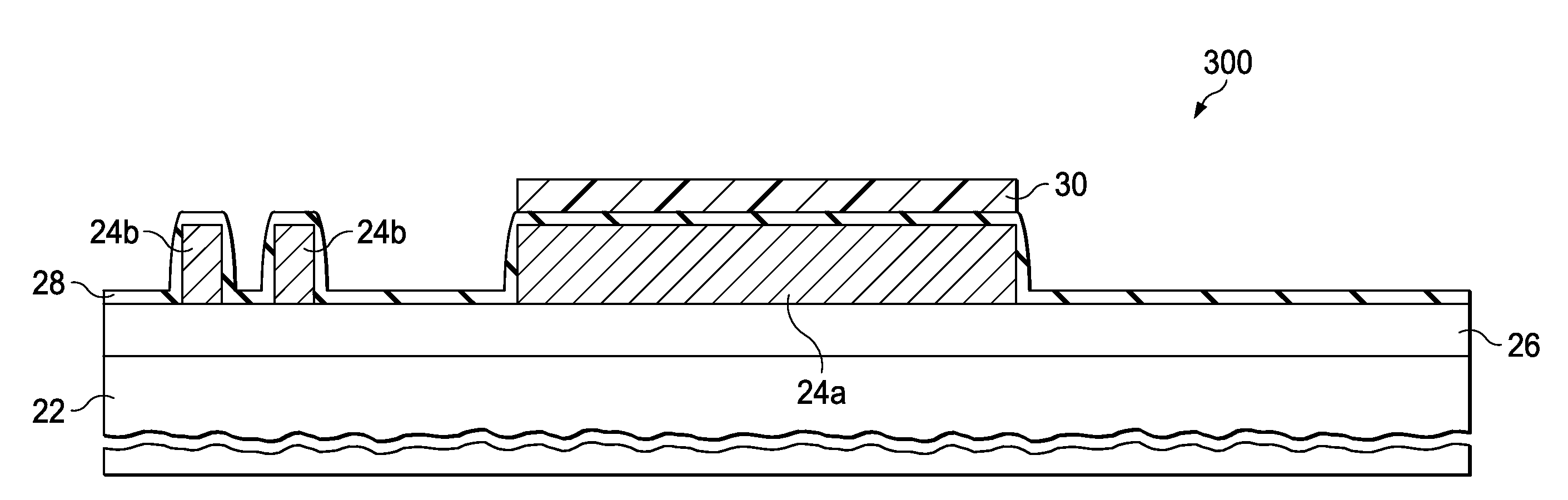
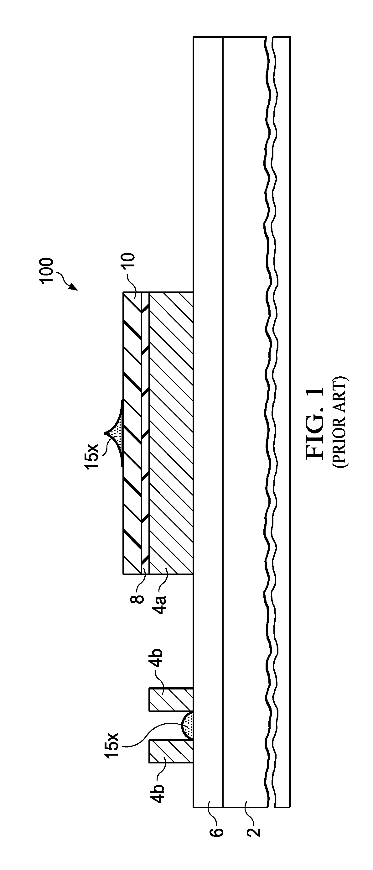
[0021]This invention will be described in connection with one or more of its embodiments, namely as implemented into a manufacturing process for fabricating a particular integrated circuit having elements formed of metal or metal compounds. However, it is contemplated that this invention may also be beneficial when applied to other processes and in connection with other applications. In particular, while an example of this invention is described in detail in connection with the fabrication of a parallel-plate capacitor in an integrated circuit, this invention is no more particularly directed to the forming of a capacitor than it is to the forming of any other integrated circuit element or structure. Accordingly, it is to be understood that the following description is provided by way of example only, and is not intended to limit the true scope of this invention as claimed.

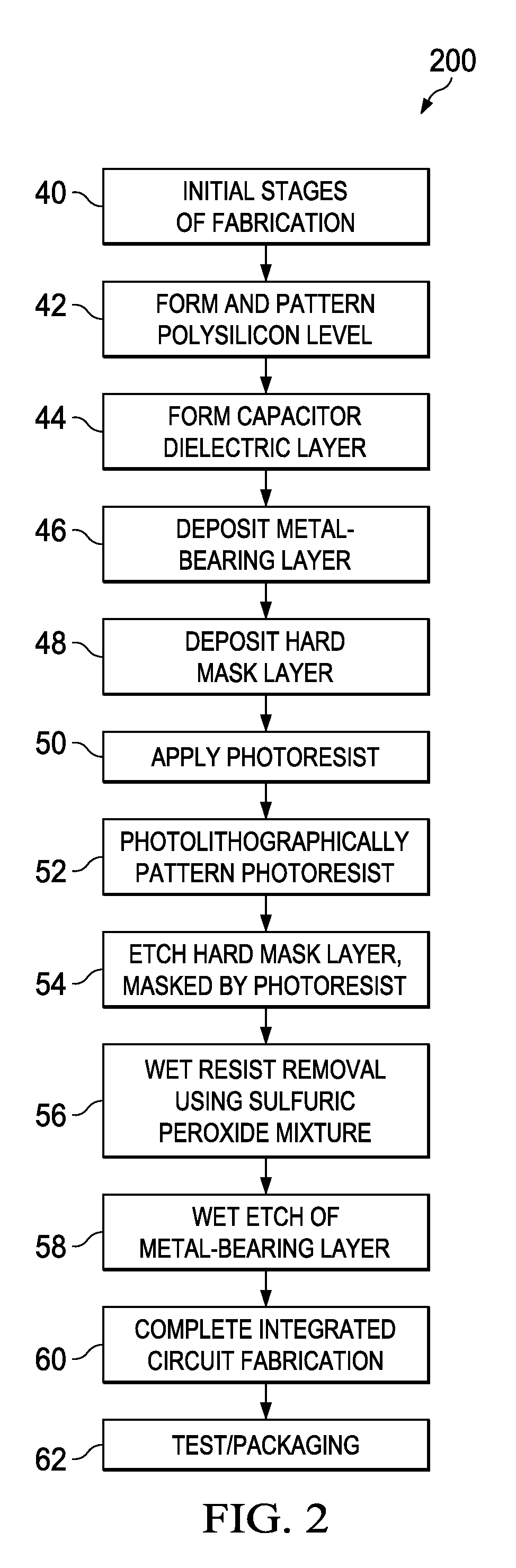
[0022]Referring now to FIG. 2, which depicts a flow chart for a process 200 for fabricating metal-bearing struct...


PUM

PropertyMeasurementUnit
temperatureaaaaaaaaaa
temperaturesaaaaaaaaaa
semiconductingaaaaaaaaaa

Abstract

A method of fabricating metal-bearing structures in an integrated circuit such as metal-polysilicon capacitors using conductive metal compounds. Defects due to organometallic polymers formed during the etch of a hard mask material are minimized by using a process that includes a plasma etch for the hard mask that achieves a predominantly chemical character using a fluorine-based etch chemistry. Using a low-temperature liquid-phase strip of the hard mask photoresist instead of an ash prevents further cross-linking of polymers formed during the plasma etch. Etching the metal-bearing material using a hot fully-concentrated mixture of ammonium hydroxide and hydrogen peroxide allows short etch times that are particularly shortened for tantalum nitride films deposited with a nitrogen concentration of about 30 percent or greater.

Description

CROSS-REFERENCE TO RELATED APPLICATIONS[0001]This Application is related to the subject matter described in U.S. patent application Ser. No. 12 / 549,538 by Raghavan, et al., filed Aug. 28, 2009, and entitled LOW TEMPERATURE SURFACE PREPARATION FOR REMOVAL OF ORGANOMETALLIC POLYMERS IN THE MANUFACTURE OF INTEGRATED CIRCUITS. That application describes a method of removing photoresist from a surface during the manufacture of an integrated circuit, which is a step in a preferred embodiment described below. Accordingly, the entire contents of U.S. patent application Ser. No. 12 / 549,538 are hereby incorporated by reference.BACKGROUND OF THE INVENTION[0002]1. Field of the Invention[0003]This invention is in the field of integrated circuit manufacture. Embodiments of this invention are more specifically directed to methods of forming metal-bearing structures having low defect density due to organometallic polymer and other residues.[0004]2. Description of the Related Art[0005]In recent year...

Claims


Application Information

Patent Timeline
Patent Type & Authority Applications(United States)
IPC IPC(8): H01L21/3205
CPCH01L21/0206H01L21/31116H01L28/40H01L21/32134H01L21/32139H01L21/31133
Inventor RAGHAVAN, SRINIVASCHERUKURI, KALYANLILLIBRIDGE, THOMAS E.FAUST, RICHARD A.
Owner TEXAS INSTR INC
Why Eureka
Try Eureka