[0011]One of the most critical issues in the design of
semiconductor photovoltaic (PV) devices stems from the difference in the optimum length scales required for collection of the photo-generated carriers and for absorption of the incoming
optical energy. In thinner structures, more photo-generated carriers can be collected before their
annihilation through recombination. On the other hand, thick structures allow the incoming lightwave to penetrate deeper and ensure a higher degree of absorption of its photons. Traditionally, optical enhancements have involved use of anti-reflecting coatings coupled with a metallic
back reflector.
Solar cell efficiencies are improved by textured metallic back reflectors which scatter incident light through oblique angles, thereby increasing the
path length of photons within the absorber layer. Such textured back reflectors exhibit intrinsic losses of light from
plasmon modes within the absorber.
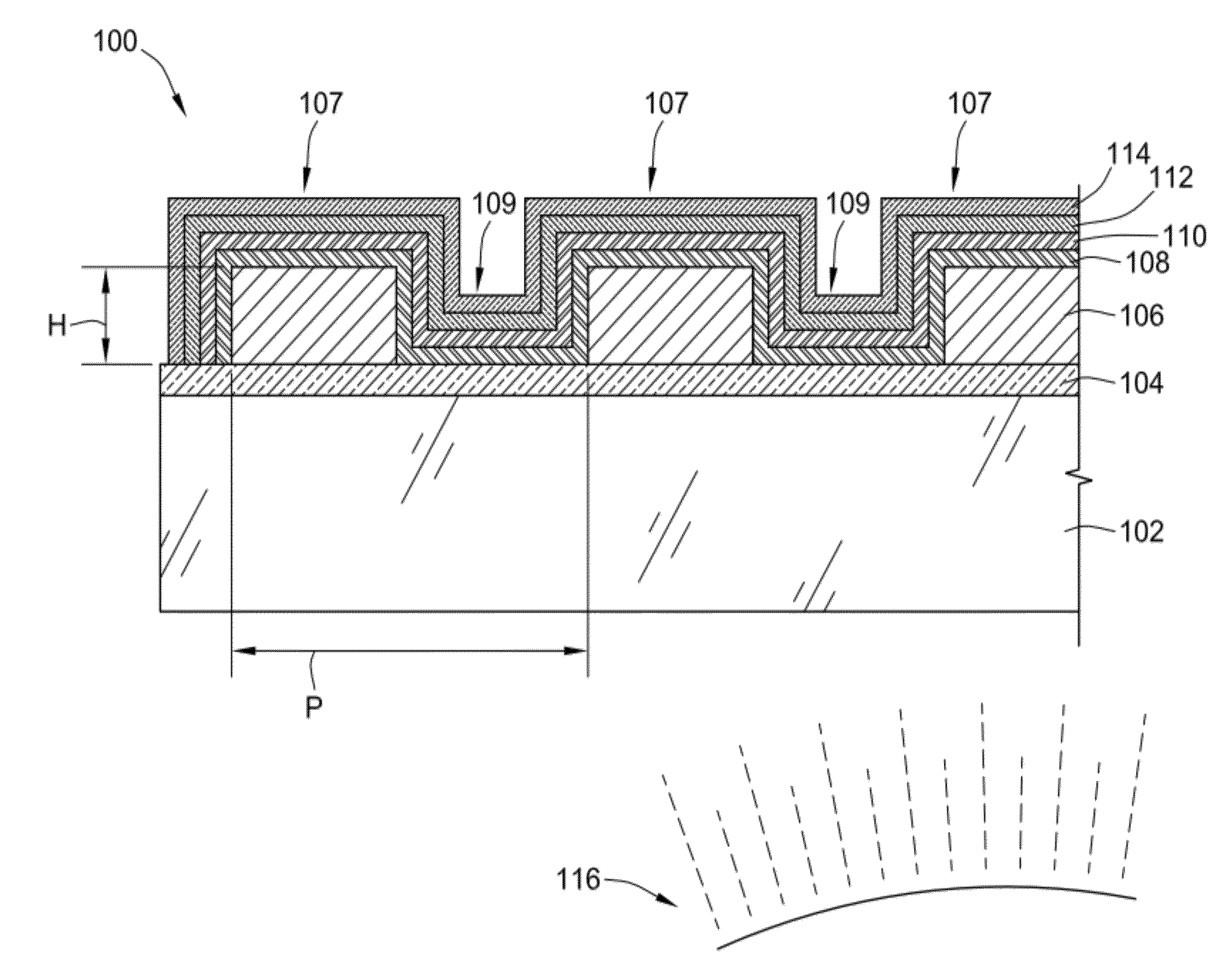
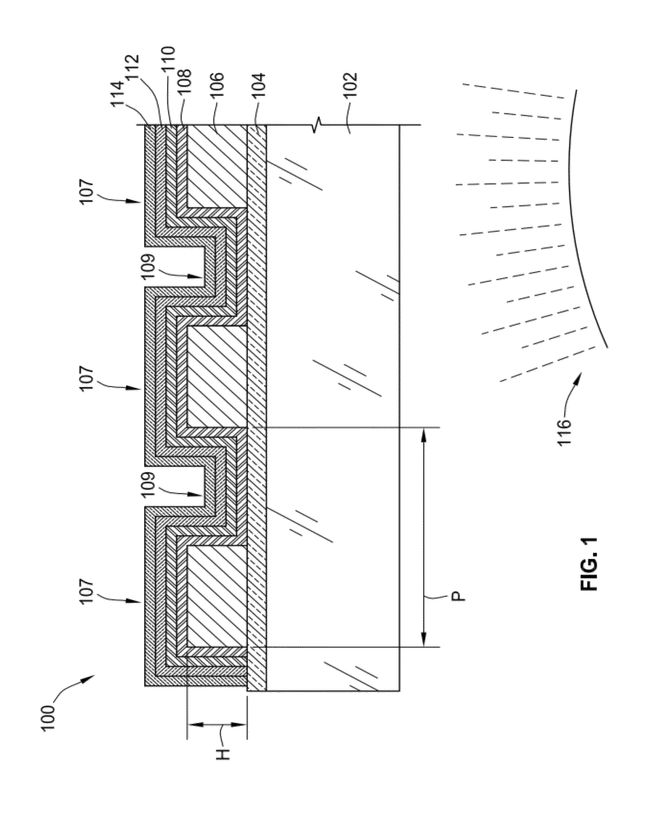
[0012]To overcome such problems, an embodiment of the present invention utilizes microscale textured, or microtextured, surfaces with tapered ends in a conceptually different way as compared with conventional back reflectors. In particular embodiments of the invention, ultrathin (e.g., less than 50 nanometers (nm))
layers of photovoltaic polymers are deposited on the microtextured and tapered electrodes. Upon encapsulation by another metallic / polymeric
electrode, this architecture leads to highly efficient photovoltaic conversion. High efficiency arises from optimized
light management in textures and tapered features on the order of the
wavelength of absorbed light, and also from optimized
electron-hole pairs and charged transport mechanisms in the ultrathin
polymer films.
[0013]Unlike the nanoscale and macroscale approaches described in the Background, the microscale light-management architecture used in embodiments of the present invention is more powerful in terms of its
efficacy for highly efficient solar cells. Due to the tapered ends of the microtextured templates,
optical energy is highly enhanced and a high degree of absorption will take place even in a very thin photoactive
organic film. This thin film will be thin enough so that
electron-hole pairs are efficiently dissociated into free charges, and these
resultant charges are efficiently transported to the
external circuit. The improvement in power conversion efficiency that this design will enable is potentially much more than the competing approaches discussed in the Background above. Due to employment of a soft-
lithography-based fabrication approach, our approach in embodiments of the invention is also scalable and relatively low-cost.
[0014]In embodiments of the present invention, the
pitch and height of the textured substrate, adequate for conformal BHJ layer
coating as well as absorption enhancement at the band edge of the
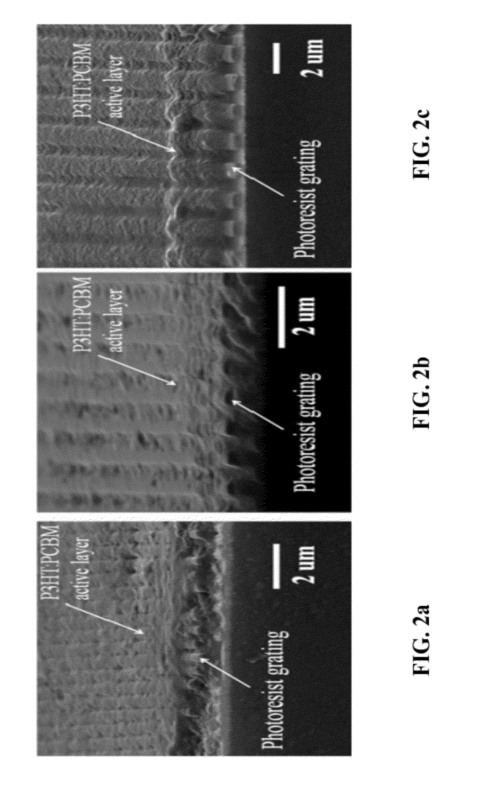
active polymer, which in one embodiment is P3HT, is controlled. Moreover, the texture is preferably provided by
photoresist lithography, which has played a key role in
semiconductor industry
microfabrication in last few decades and has undergone immense development to reduce
processing cost and improve
scalability, making this process viable for large scale production of grating based OSCs.
[0015]In some embodiments of the present invention, average doubling of absorption near the band edge (600 nm≦λ≦700 nm) of P3HT:PCBM due to the grating geometry is achieved. Efficiency improvements of 20%, which is ascribed to light
trapping effect of these PR cells, is also achieved.

