Fine-processing agent and fine-processing method

a technology of fine-processing agent and fine-processing method, which is applied in the direction of basic electric elements, electrical apparatus, chemistry apparatus and processes, etc., can solve the problems of high foaming ability, difficult to achieve desired shape, and unsuitable for semiconductor device manufacturing processes, etc., and achieve low etching controllability

Active Publication Date: 2012-03-08
STELLA CHEMIFA CORP
View PDF6 Cites 8 Cited by
  • Summary
  • Abstract
  • Description
  • Claims
  • Application Information

AI Technical Summary

Benefits of technology

[0027]The invention produces the advantageous effects as described below by the means described above.
[0028]Specifically, when a laminated film composed of at least a silicon oxide film and a silicon nitride film is subjected to fine processing, the invention makes possible selective fine processing of only the silicon oxide film, so that successful fine processing can be achieved, for example, in the manufacture of semiconductor devices, liquid crystal display devices, micromachine devices, etc.EMBODIMENTS FOR CARRYING OUT THE INVENTION
[0030]A fine processing agent according to an embodiment of the invention contains (a) at least one of hydrogen fluoride or ammonium fluoride, (b) water, and (c) a water-soluble polymer.
[0031]The content of hydrogen fluoride as the component (a) is preferably in the range of 0.01 to 15% by weight, more preferably in the range of 0.05 to 10% by weight, based on the total weight of the fine processing agent. If the hydrogen fluoride content is less than 0.01% by weight, it will be difficult to control the hydrogen fluoride concentration so that there may be significant variations in the etch rate for a silicon oxide film. If the hydrogen fluoride content is more than 15% by weight, the etch rate for a silicon oxide film will be too high so that the etching controllability may be low.
[0032]The content of ammonium fluoride is preferably in the range of 0.1 to 40% by weight, more preferably in the range of 5 to 25% by weight, based on the total weight of the fine processing agent. If the ammonium fluoride content is less than 0.1% by weight, it will be difficult to control the ammonium fluoride concentration so that there may be significant variations in the etch rate for a silicon oxide film. If the ammonium fluoride content is more than 40% by weight, it will be close to the saturation solubility of ammonium fluoride so that a reduction in the liquid temperature of the fine processing agent may lead to the attainment of the saturation solubility of the fine processing agent to cause crystal precipitation in the liquid.
[0033]In an embodiment of the invention, the addition of the component (a) makes it possible to selectively reduce the etch rate for a silicon nitride film so that high etching selectivity (silicon oxide film / silicon nitride film) can be achieved. More specifically, when the component (a) is added, for example, the etch rate for a silicon nitride film can be reduced to 80% or less of that obtained when the component (a) is not added.

Problems solved by technology

As a result, patterning into the desired shape becomes difficult.
Unfortunately, such a fine processing agent has very high foaming ability and therefore is not suitable for use in semiconductor device manufacturing processes.
However, the reduction in the thickness of a silicon oxide film as a capacitor insulating film has reached a limit for 1 Mbit DRAM.
The problem described below occurs when a conventional etchant is used in a process that includes forming cylindrical capacitor lower electrodes and then removing the formed silicon oxide film by wet etching to form a capacitor.
The drying process has the problem that due to the surface tension of water present between the capacitor lower electrodes, a “leaning” phenomenon, in which the lower electrodes lean and come into contact with each other, frequently occurs to induce 2-bit failure.
In these semiconductor device manufacturing processes, the use of a conventional etchant has the problem that the silicon oxide film disclosed as a support film in Patent Document 1, the silicon nitride film disclosed in Patent Document 2, or the silicon oxide film disclosed as an etching stopper film in Patent Document 3 is also etched together with the etching target.

Method used


Image

  • Fine-processing agent and fine-processing method
  • Fine-processing agent and fine-processing method

Examples


example 1

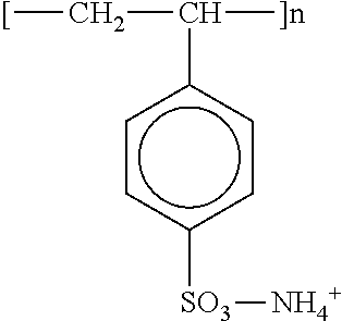
[0053]A solution of a mixture of 7.0 parts by weight of hydrogen fluoride (high-purity grade for semiconductor applications, 50% by weight in concentration, manufactured by Stella Chemifa Corporation), 50.0 parts by weight of ammonium fluoride (high-purity grade for semiconductor applications, 40% by weight in concentration, manufactured by Stella Chemifa Corporation), and 40.5 parts by weight of ultrapure water was prepared, and 2.5 parts by weight of poly(ammonium acrylate) (6,000 in weight average molecular weight, 40% by weight in concentration) as a water-soluble polymer was added to the solution. After mixing and stirring, the liquid mixture was adjusted to a temperature of 25° C. and allowed to stand for 3 hours. Thus, an etchant (a fine processing agent) was prepared which contained 3.5% by weight of hydrogen fluoride, 20.0% by weight of ammonium fluoride, and 1% by weight of poly(ammonium acrylate).

[0054]Subsequently, etch rates were measured for a TEOS film, as a silicon o...

examples 2 to 10

[0055]In Examples 2 to 10, etchants were prepared as in Example 1, except that the contents of hydrogen fluoride and ammonium fluoride and the type and content of the water-soluble polymer were changed as shown in Table 1. Using the etchant obtained in each example, etch rates for a TEOS film and a silicon nitride film, and etch rate selectivity (silicon oxide film / silicon nitride film) were also evaluated. The results are shown in Table 2 below.

example 11

[0060]A solution of a mixture of 20.0 parts by weight of hydrogen fluoride (high-purity grade for semiconductor applications, 50% by weight in concentration, manufactured by Stella Chemifa Corporation), 27.8 parts by weight of hydrochloric acid (electronic industry grade, 36% by weight in concentration, manufactured by HAYASHI PURE CHEMICAL IND., LTD.), and 51.2 parts by weight of ultrapure water was prepared, and 1.0 part by weight of polyacrylamide (10,000 in weight average molecular weight, 50% by weight in concentration) as a water-soluble polymer was added to the solution. After mixing and stirring, the liquid mixture was adjusted to a temperature of 25° C. and allowed to stand for 3 hours. Thus, an etchant (a fine processing agent) was prepared which contained 10% by weight of hydrogen fluoride, 10% by weight of hydrochloric acid, and 0.5% by weight of polyacrylamide.

[0061]Subsequently, etch rates were measured for a BPSG film, as a silicon oxide film, and a silicon nitride fi...


PUM

PropertyMeasurementUnit
liquid temperatureaaaaaaaaaa
concentrationaaaaaaaaaa
temperatureaaaaaaaaaa

Abstract

Provided is a fine-processing agent which, when fine-processing a laminated film stacked at least with a silicon dioxide film and a silicon nitride film, can selectively fine-process the silicon dioxide film. Also provided is a fine-processing method utilizing the fine-processing agent. The fine-processing agent is characterized by including: (a) 0.01-15.0 weight % hydrogen fluoride and / or 0.1-40.0 weight % ammonium fluoride, (b) water, and (c) 0.001-10.00 weight % water-soluble polymer selected from among a group consisting of acrylic acid, ammonium acrylate, acrylic acid ester, acrylamide, styrenesulfonic acid, ammonium styrenesulfonate, and styrenesulfonic acid ester.

Description

TECHNICAL FIELD[0001]The invention relates to a fine processing agent for use in fine processing, cleaning, or other processes in the manufacture of semiconductor devices, liquid crystal display devices, micromachines (micro electro mechanical systems (MEMS)) devices, etc., and to a fine processing method using such an agent. In particular, the invention relates to a fine processing agent for use in fine processing of a laminated film in which at least a silicon oxide film and a silicon nitride film are laminated, and to a fine processing method using such an agent.BACKGROUND ART[0002]Among semiconductor device manufacturing processes, one of the most important processes is patterning and etching of a silicon oxide film, a silicon nitride film, a polysilicon film, a metal film, or any other film formed on the surface of a wafer into the desired shape. Wet etching, one of such etching techniques, has required a fine processing agent capable of selectively etching only an etching targ...

Claims


Application Information

Patent Timeline
Patent Type & Authority Applications(United States)
IPC IPC(8): C09K13/00C09K13/08
CPCH01L21/31111C09K13/08H01L21/306
Inventor MIYASHITA, MASAYUKIKUJIME, TAKANOBUNII, KEIICHI
Owner STELLA CHEMIFA CORP
Why Eureka
Try Eureka