Device having self-assembled-monolayer

a monolayer, self-assembling technology, applied in the direction of instruments, biological material analysis, coatings, etc., can solve the problems of bio-sensing devices subject to potentially conflicting design choices, catastrophic device failure, and degradation of device performance, so as to prevent corrosion inhibition, effective corrosion inhibition, and copper protection properties

Inactive Publication Date: 2012-04-12
NXP BV
View PDF2 Cites 50 Cited by
  • Summary
  • Abstract
  • Description
  • Claims
  • Application Information

AI Technical Summary

Benefits of technology

[0021]In embodiments, R1 comprises an alkyl, alkenyl, cyclic alkyl, aryl, alkyl bound to aryl, alkenyl bound to aryl or alkynyl bound to aryl. In a particularly preferred embodiment, R1 is an alkyl group. In the case that the alkyl chain has no side chains it is particularly suited for close packing and thereby it provides an effective barrier between the terminal group of the SAM and the copper electrode to limit or even prevent corrosion inhibition and thus to pro...

Problems solved by technology

Conventional semiconductor devices normally are designed and packaged to exclude moisture, liquid and oxygen, since it is well known that moisture, liquid or oxygen can oxidise the materials of the device, in particular metallic contact materials, and thereby degrade the device performance and even result in catastrophic device failure.
Also, bio-sensing devices may be the subject of potentially conflicting design choices.
Unfortunately, though, gold is not semiconductor compatible—at least not as far as the overwhelmingly most commonly used semiconductor, silicon, is concerned.
Its diffusion into silicon creates deep levels in the silicon band gap which damages the carrier (electron and hole) properties of silicon-base semiconductor materials.
Partly as a result, there is interest in developing SAMs for use on copper electrodes, despite the fact the copper is less convenient than gold.
However, the disadvantage of copper is that copper oxidizes very easily in saline solutions, which are often used in biosensin...

Method used


Image

  • Device having self-assembled-monolayer
  • Device having self-assembled-monolayer
  • Device having self-assembled-monolayer

Examples


Embodiment Construction

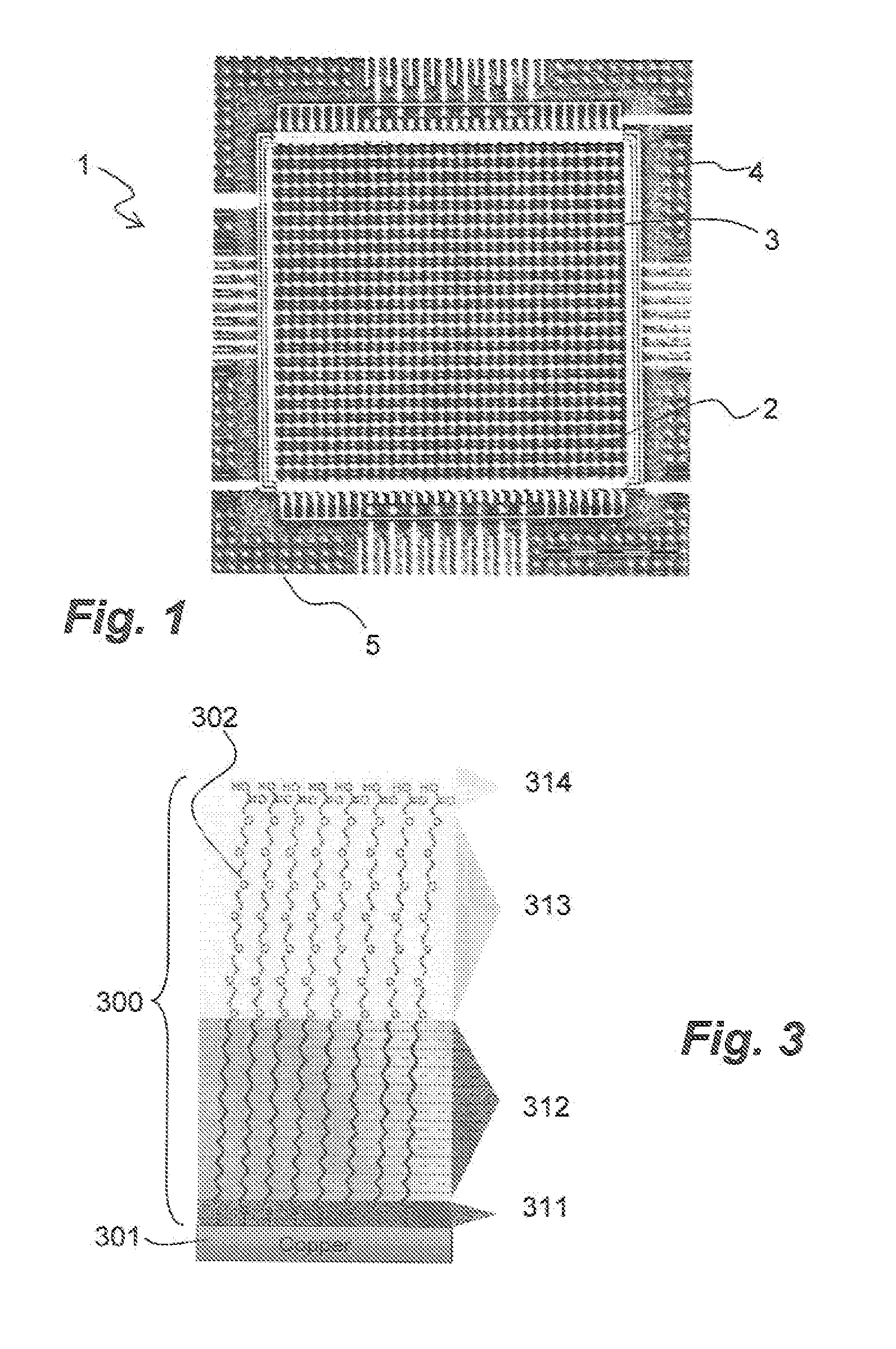
[0038]An idealised schematic plan view of a semiconductor chip for use in bio-sensing applications is shown in FIG. 1. The chip 1 comprises an array 3, in this case a Cartesian x-y array, of individual sensor electrodes 2, which is surrounded by peripheral region 4 where copper dummies are buried in the silicon oxide 5. In use (not shown in this figure) microfluidic channels are provided which allow for a fluid to flow over the surface of the chip. In bio-sensing applications, the fluid may carry, in solution or suspension, target bio-molecules. The copper nano / microelectrode can bind the receptor biomolecules capable of binding the target biomolecules in the fluid.

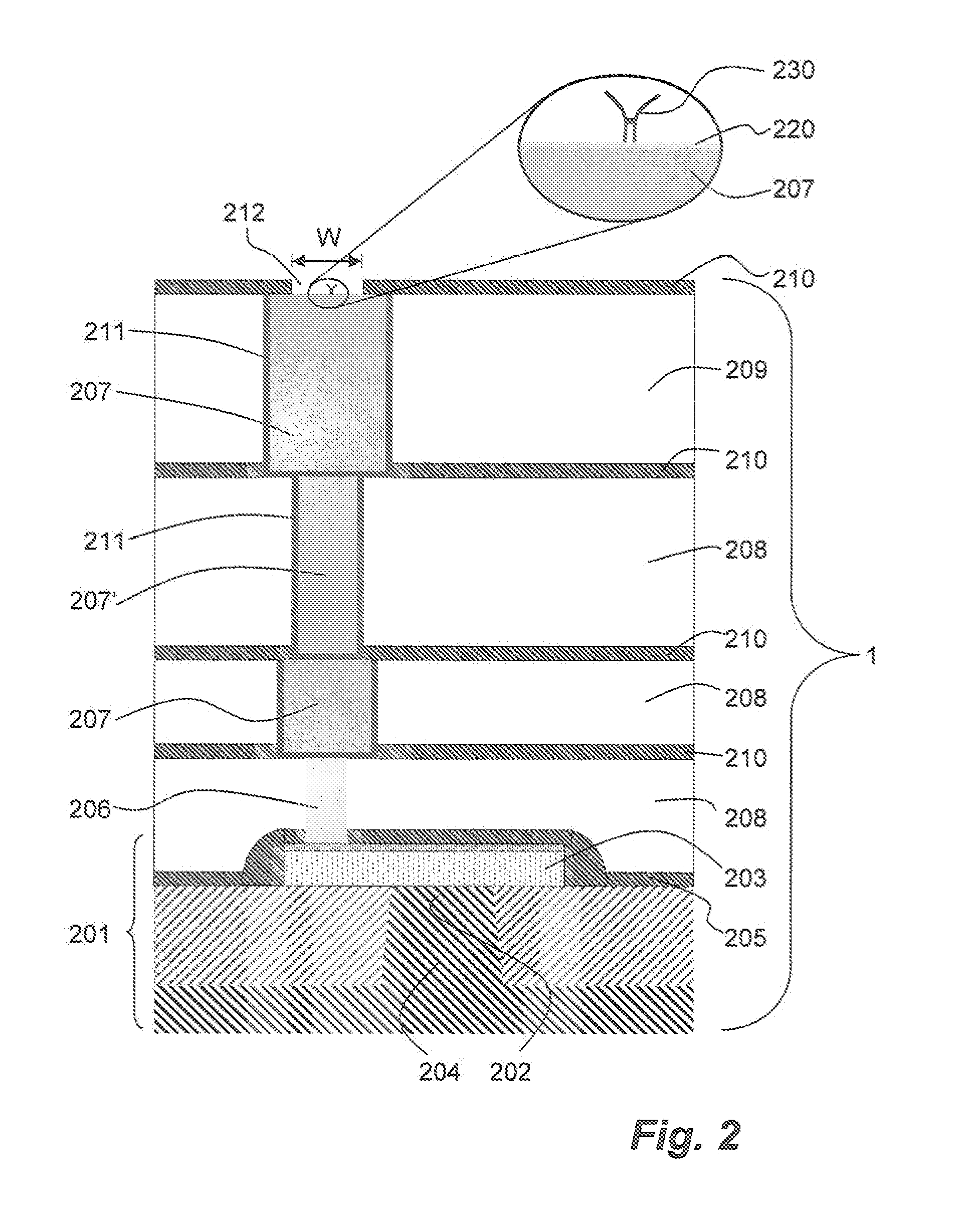
[0039]FIG. 2 shows a schematic cross-section of a part of a semiconductor chip as shown in FIG. 1. The chip 1 includes a conventional transistor MOSFET 201 comprising a channel 202, in an n-well or a p-well 204 and underneath a polysilicon gate 203. The gate oxide between the channel and the gate is not shown in the figur...


PUM


Abstract

A device for bio-sensing applications is disclosed, comprising a substrate such as a semiconductor chip having Cu electrodes thereon, and a self assembled monolayer bonded to at least one of the Cu electrodes, wherein molecules of the self-assembled monolayer comprise a head group which bonds to Cu, a carbon-comprising chain comprising a chain of at least 12 C atoms, and a terminal group which is hydrophilic and for binding a bio-receptor. The terminal group is hydrophilic to allow binding to the bio-receptor, and inclusion of the carbon-comprising chain, limits or avoids corrosion of the copper. Also disclosed is a method of providing such a device, activating the terminal group and coupling a bio-receptor to the activated terminal group. Disclosure further extends to use of such a device for bio-sensing applications.

Description

FIELD OF THE INVENTION[0001]This invention relates to devices comprising substrates such as semiconductor chips having copper electrodes with self-assembled monolayers bonded thereto, and is particularly related to such devices which are intended for bio-sensing applications. It further relates to methods of manufacturing such devices, and to uses of such devices.BACKGROUND OF THE INVENTION[0002]Recently, the present Applicant has disclosed a bio-sensing device, based on capacitive (or resistive or inductive—in general impedance) sensing of a bio-molecule, which bio-molecule is mechanically coupled to a micro-electrode. (Patent Application Publication WO-A-2009-047703). The device is particularly suited to miniaturisation and can be integrated both with conventional semiconductor technology and with micro-fluidic technology for efficient, high sensitivity and rapid throughput bio-sensing.[0003]In order to bind the target bio-molecule (e.g. viruses, DNA, RNA, proteins, antigen, pepti...

Claims


Application Information

Patent Timeline
IPC IPC(8): G01N33/566B05D5/12G01N30/00
CPCG01N33/5438G01N2610/00G01N33/553
Inventor MERELLE, THOMASLAMBERT, MAGALI HUGUETTE ALICEFREDERIX, FILIP
Owner NXP BV
Why Eureka
Try Eureka