Oscillator having negative resistance element
a resistance element and oscillator technology, applied in the field of oscillators, can solve the problems of limiting the improvement of power conversion efficiency, and achieve the effect of reducing the service life and the gain of the elemen
- Summary
- Abstract
- Description
- Claims
- Application Information
AI Technical Summary
Benefits of technology
Problems solved by technology
Method used
Image
Examples
embodiment 1
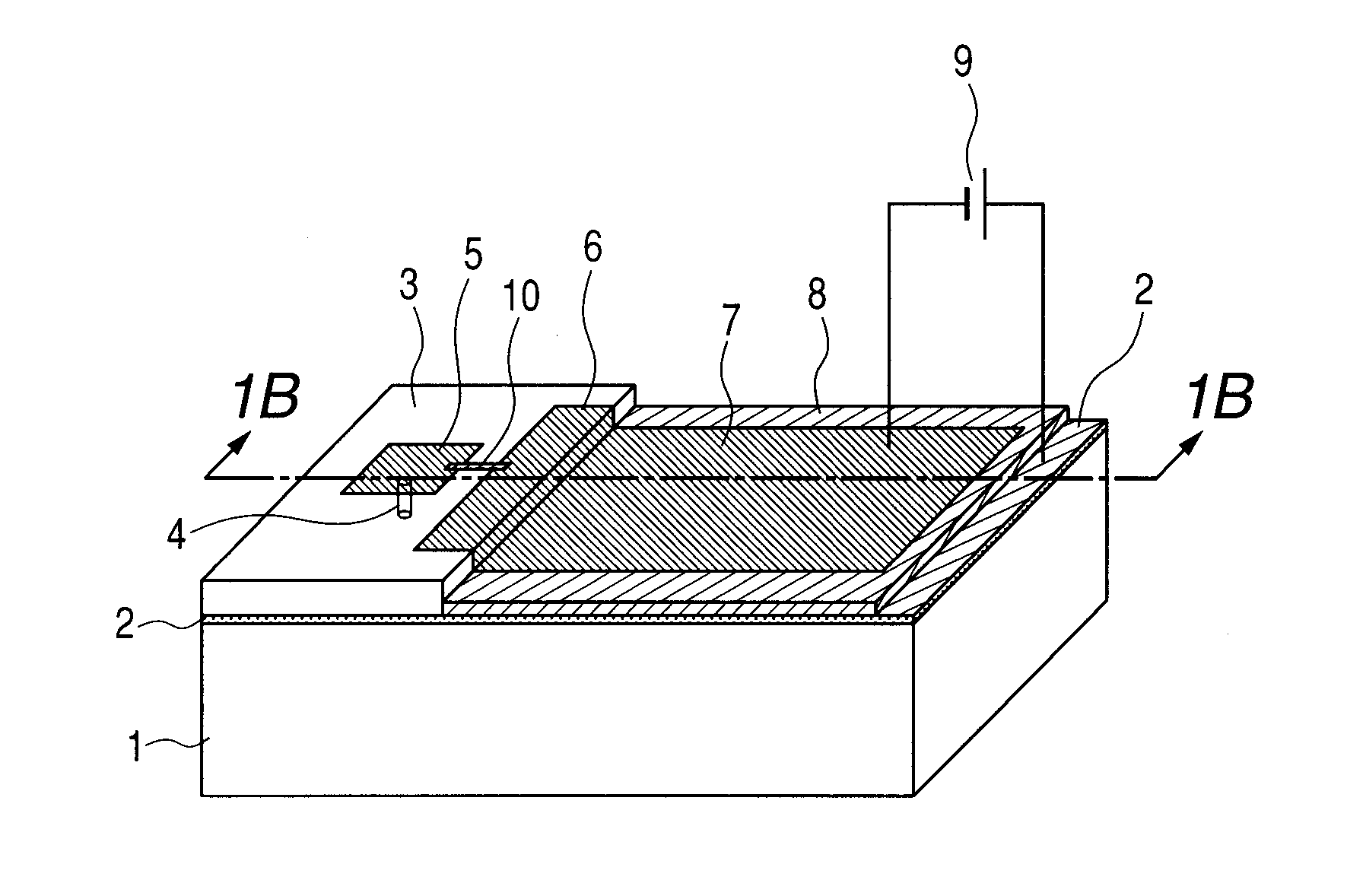
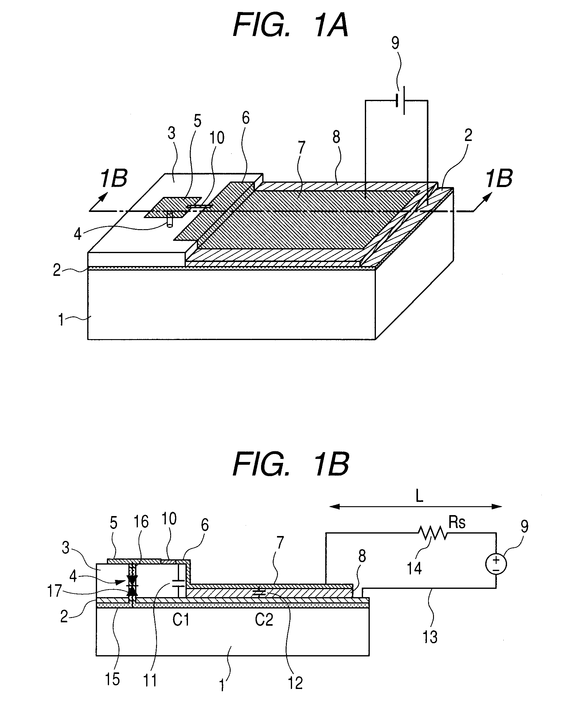
[0023]Embodiment 1 of the present invention has a structure formed by integrating an RTD element and a large capacitance capacitor on a same substrate. FIGS. 1A and 1B illustrate the structure thereof, of which FIG. 1A is a schematic perspective view and FIG. 1B is a schematic cross-sectional view taken along 1B-1B in FIG. 1A. In FIGS. 1A and 1B, 4 denotes a post-shaped RTD element and the structure further includes epitaxial layers including an InGaAs / AlAs or InGaAs / InAlAs quantum well 17, a pair of contact layers 15, 16 and spacer layers (not illustrated) formed on an InP substrate 1 by crystal growth thereof. A negative resistance element formed by using a III-V group compound semiconductor such as AlGaAs / GaAs on a GaAs substrate and AlGaN / InGaN on a GaN substrate, a IV group semiconductor such as Si / SiGe on an Si substrate, and a II-VI group semiconductor may also be applicable.
[0024]The resonator is formed by an electrode 2 that also operates as a ground plane, an electrode 5 t...
example 1
[0036]A specific example of arrangement of elements of Embodiment 1 will be described below. In this example, an RTD element is formed on an InP substrate. A triple barrier quantum well structure having a first barrier layer AlAs (1.3 nm), a first quantum well layer InGaAs (7.6 nm), a second barrier layer InAlAs (2.6 nm), a second quantum well layer InGaAs (5.6 nm), a third barrier layer AlAs (1.3 nm) is employed. All the composition ratios are lattice-matched to the InP substrate except AlAs. On the other hand, AlAs is a strained layer but the thickness is less than the critical film thickness. A spacer layer made of non-doped InGaAs, an n-type InGaAs electric contact layer and an n+InGaAs contact layer are arranged at the top and also at the bottom of the triple barrier quantum well structure. The RTD element post is circular with a diameter of about 2 μm. Then, current voltage characteristics including a current density of Jp=280 kA / cm2, a peak valley ratio of 3 and a differentia...
embodiment 2
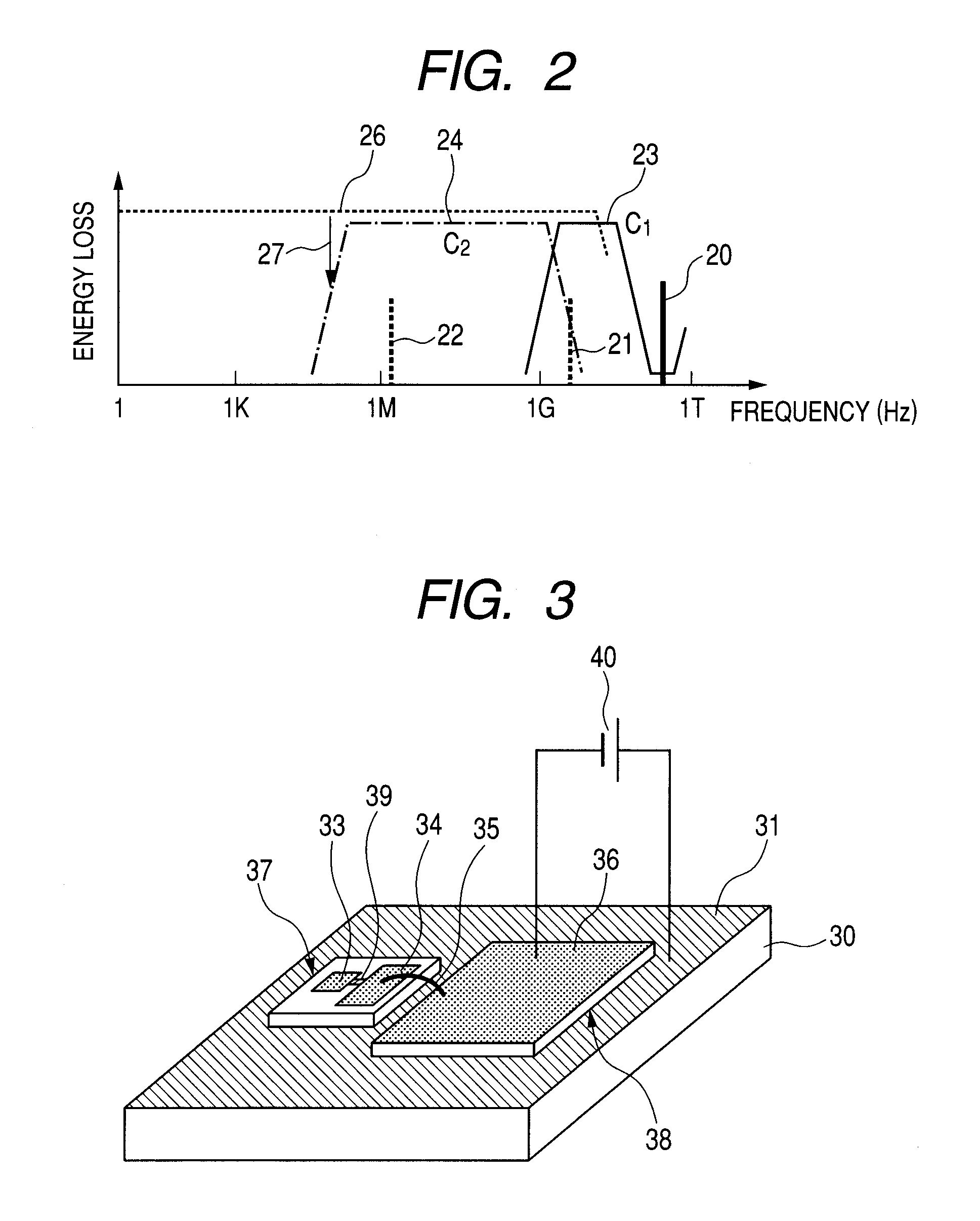
[0038]Embodiment 2 of the present invention has such a structure that a second capacitor is installed on a same mount as a separate chip as illustrated in FIG. 3. In FIG. 3, 30 denotes a sub-carrier for installing the chips. A substrate prepared by coating an electroconductive layer 31 such as Au on a ceramic substrate such as Si substrate, Al2O3 and AlN or on a plastic substrate or a metal plate may selectively be employed for the sub-carrier 30. 37 denotes an RTD element chip or a single chip realized to carry the RTD element and components down to the part that corresponds to the first capacitor of Embodiment 1. A patch antenna 33 and an electrode 34 are connected by a line 39. Note, however, that the capacitance of the part that corresponds to the first capacitor needs to be made larger than that of Embodiment 1. One of the contacts of the RTD element is connected to the electroconductive layer 31 of the sub-carrier and the other contact is connected to one of the electrodes (36...
PUM
 Abstract
Description
Claims
Application Information


