Optical Device

a technology of optoelectronic devices and optical devices, applied in the direction of solid-state devices, electrical devices, photovoltaic energy generation, etc., can solve the problems of further constraints on design, impact cost, and pitaxial defects in conventional, point, thread and dislocation defect types, so as to simplify optical design of structures, reduce angular cones, and high directionality

Active Publication Date: 2012-05-10
UNIV OF SOUTHAMPTON
View PDF3 Cites 55 Cited by
  • Summary
  • Abstract
  • Description
  • Claims
  • Application Information

AI Technical Summary

Benefits of technology

[0073]Furthermore, in a conventional PC-LED device where the overall epitaxial thickness is several microns, then tens or even hundreds of modes contribute towards the overall radiated far field profiles. In the present invention the number of modes contributing to or involved in the emission process (or collection for light harvesting) is limited or determined by the depth and width of the enclosing shaped structures, thereby simplifying optical design of the structures and allowing unusual beam patterns to be easily obtained. In the case of a light emitting device, such beam patterns could include high directionality (reduced angular cone), uniform intensity far fields or structured far field patterns such as extreme bat-wings. Such beam profiles are beneficial for applications such as display and general lighting.
[0074]A significant advantage of the devices of the present invention is that the upper surface of the device may be coated with an optically opaque metal contact layer with the shaped cavity structures disposed through this top contact layer and the underlying heterostructure. In contrast to conventional LEDs and OLED devices, this allows the top contact stack to be arbitrarily designed, in terms of material used, to minimise contact resistance to the underlying heterostructure, thereby providing means of improvement

Problems solved by technology

Epitaxial defects in conventional LEDs can include point, thread and dislocation defect types.
To reduce defect density the epitaxial layers must be matched in lattice constant to an underlying substrate material which further places constraints on their design and impact cost.
Non-transparent metal contact stacks are then deposited onto this which subsequently mask part of the light emitting area and thus reduce efficiency of the device.
Sapphire (which is well lattice matched to GaN) is a poor heat conductor and so such devices of this design suffer reduced lifetimes, if driven at the very high current densities which are required for general lighting applications.
Additionally, the necessity for a thin optically transparent top current spreading layer places constraints on the achievable contact resistance, and therefore on electrical efficiency of the device.
A key intrinsic problem for conventional LEDs is the issue of poor light extraction efficiency.
Due to the relatively high refractive index of common semiconductor materials combined with the fact that light is generated deep within the epitaxial structure, Fresnel reflection at the semiconductor/air interface causes confinement of a large proportion of the radiated energy.
This factor severely limits the wall plug efficiency for conventional LEDs.
In both cases the positions of the random structures are seeded by epitaxial defect sites, and hence this technique is not compatible or beneficial with very high quality low defect density epitaxy.
Photons incident upon the phosphors are therefore subject to further Fresnel reflection which again severely inhibits the efficiency of photon absorption to the phosphor.
Hence the efficiency of the overall process is still quite low.
In addition it is very difficult to find phosphors with all the correct properties to cover certain colour ranges, and so the wallplug

Method used


Image

  •  Optical Device
  •  Optical Device
  •  Optical Device

Examples


first embodiment

of a Light Harvesting Device Incorporating a p-n Junction

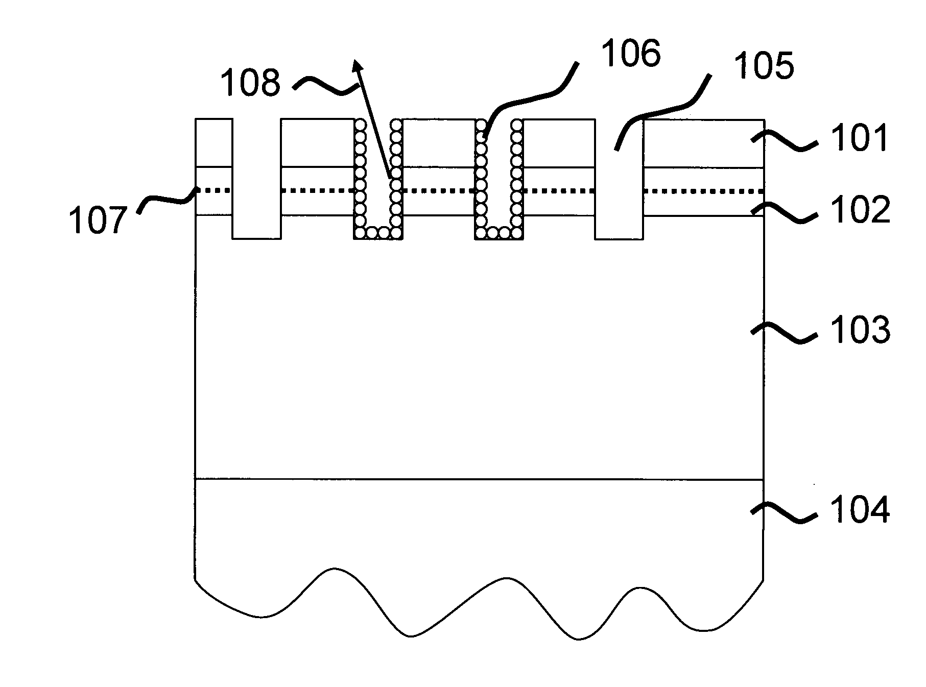
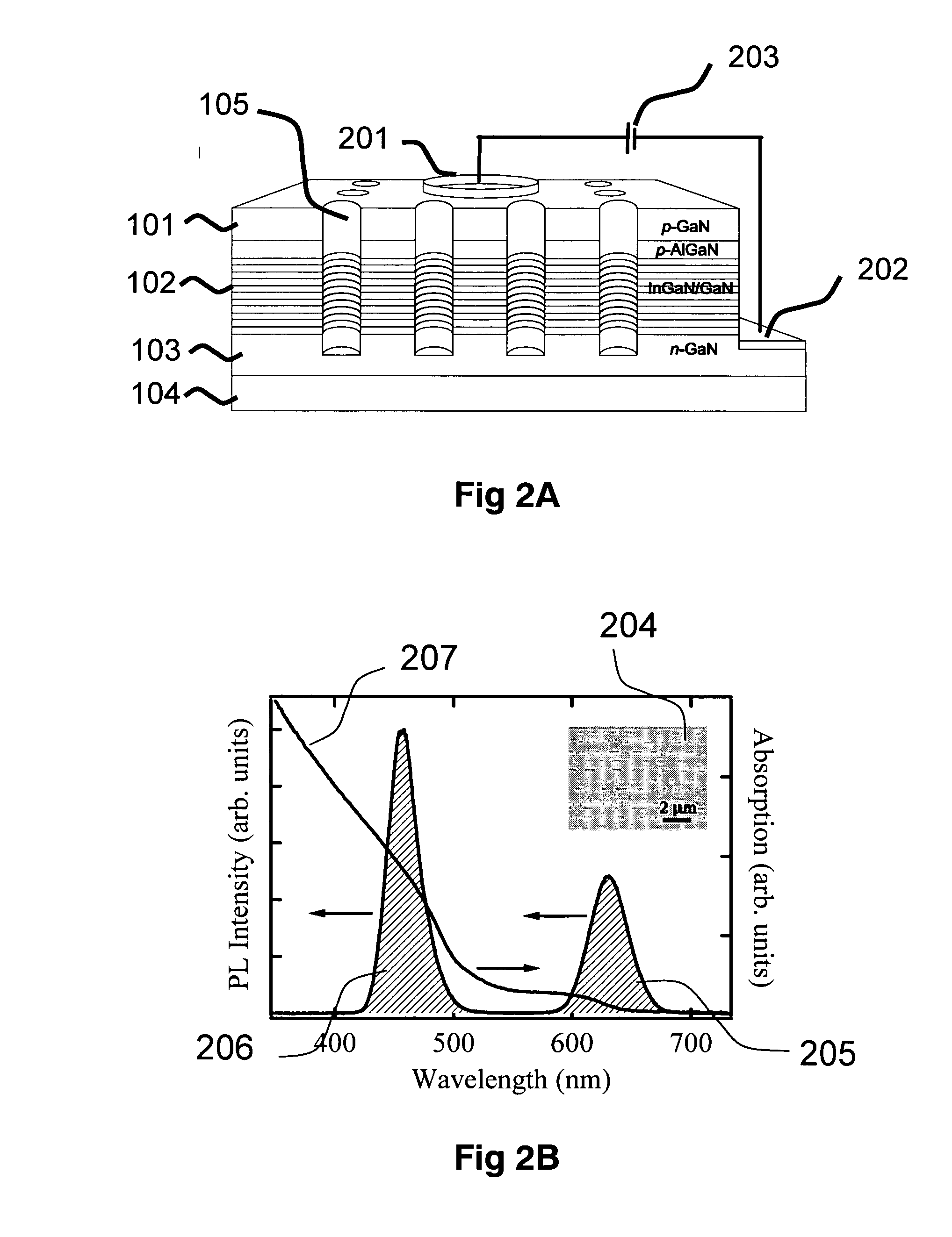
[0161]For purpose of example we now discuss in detail the practical implementation and demonstration of the first embodiment of the present invention as a light harvesting device with reference to the figures whereby the composite enclosing structure incorporates a single p-i-n junction as the energy transfer region in a configuration, leading to strong enhancement of the measured photocurrent. The excited state energy of the deposited NCs is efficiently transferred to a patterned bulk heterostructure by means of nonradiative energy transfer. Electron-hole pairs transferred to the heterostructure are subsequently separated by the built-in electric field and are collected by the electrodes resulting in electrical current.

[0162]The semiconductor bulk heterostructure used in this example offers higher carrier transport than the QW heterostructure in the previous example. In this configuration, wide absorption range and high oscil...

second embodiment

of the Invention

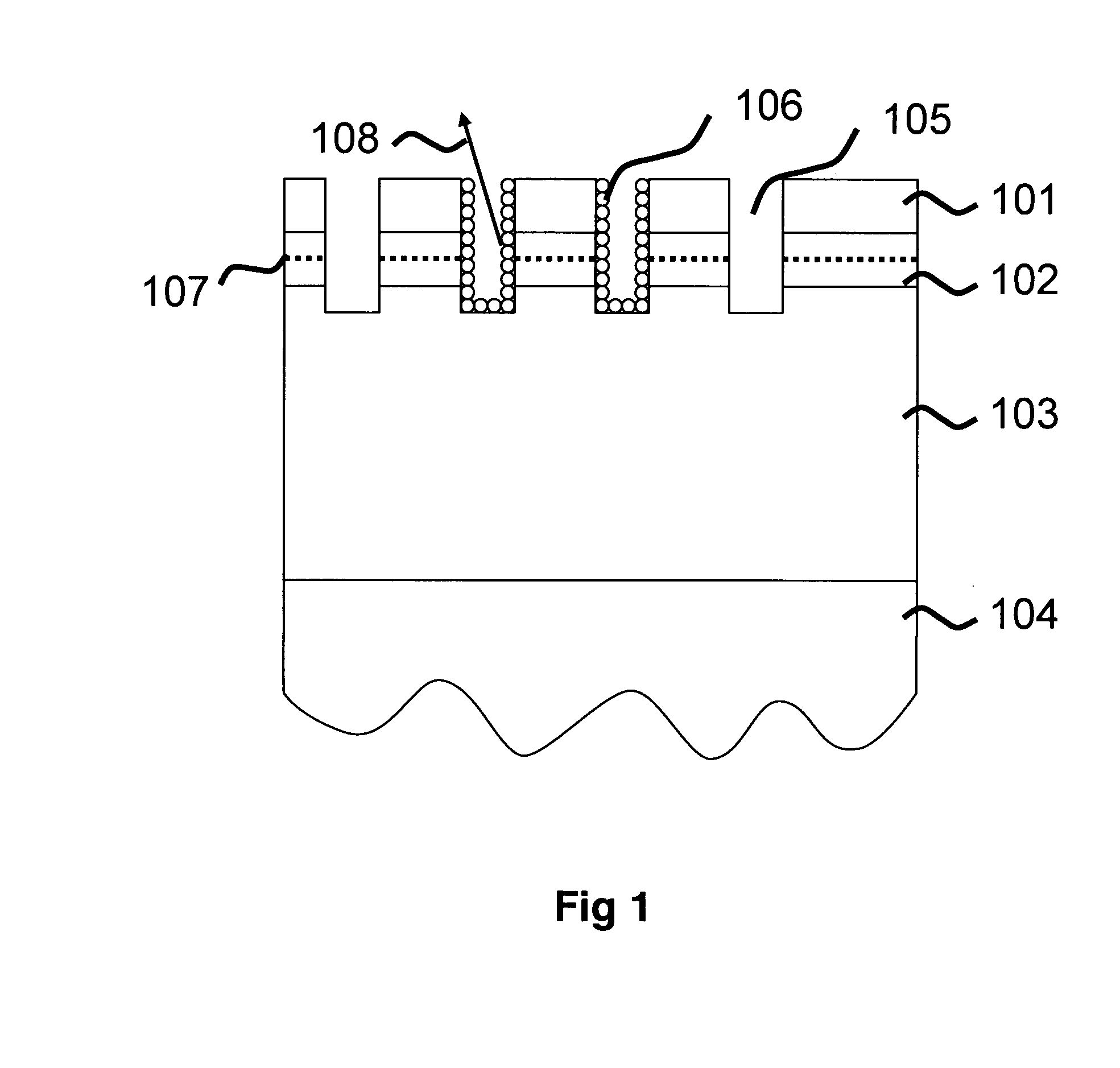
[0171]In a second embodiment of the invention (where the refractive index of the enclosing structure shown in FIG. 1 (101-103) is larger than that of the shaped structures shown in FIG. 1 (105), a large proportion of emitted light becomes reflected back from the side walls of the shaped structures, due to Fresnel reflection at the low to high refractive index boundary at the surface interface, such that each shaped structure acts predominantly as a reflective cavity for light emitted from (or collected by) the light emitting (or light absorbing) particle providing further beneficial effects as will now be described.

[0172]FIG. 13 shows in more detail the process of light emission from the optically responsive particle under such circumstances. A light ray (1301) emitted from a optically responsive particle (106) placed in close proximity to the energy transfer region (107), radiating towards the direction of the proximal heterostructure, becomes predominantly reflecte...

third embodiment

of the Invention

[0189]In a third embodiment of the invention, the enclosing structure incorporates a number of energy transfer regions perforated by a shaped structure (FIG. 21) such that more than one energy transfer region (2101) participates in the non-radiative energy transfer process to or from the colloidal nanoparticles. In this embodiment of the invention emission power (brightness), or collection efficiency, scales with number of perforated quantum wells.


PUM


Abstract

An improved optoelectronic device is described, which employs optically responsive nanoparticles and utilises a non-radiative energy transfer mechanism. The nanoparticles are disposed on the sidewalls of one or more cavities, which extend from the surface of the device through the electronic structure and penetrate the energy transfer region. The nanoparticles are located in close spatial proximity to an energy transfer region, whereby energy is transferred non-radiatively to or from the electronic structure through non-contact dipole-dipole interaction. According to the mode of operation, the device can absorb light energy received from the device surface via the cavity and then transfer this non-radiatively or can transfer energy non-radiatively and then emit light energy towards the surface of the device via the cavity. As such, the deice finds application in light emitting devices, photovoltaic (solar) cells, displays, photodetectors, lasers and single photon devices.

Description

FIELD OF THE INVENTION[0001]The present invention relates to improved optoelectronic devices which employ optically responsive nanoparticles and utilise a non-radiative energy transfer mechanism, and particularly to practical device configurations for improving the efficiency of operation. Such devices include light emitting devices, photovoltaic (solar) cells, displays, photodetectors, lasers and single photon devices.BACKGROUND TO THE INVENTION[0002]In view of raised global awareness of the depletion of non-renewable energy sources and the associated impact on the environment there is intense interest and highly focused efforts to develop green, renewable energy technologies, and increase the wall plug efficiency of existing technologies where possible.[0003]Approximately 19% of the world's energy consumption is currently attributed to lighting. Present lighting technologies include incandescent lamps, fluorescent lamps, Light Emitting Diodes and Organic Light Emitting Diodes. Var...

Claims


Application Information

Patent Timeline
IPC IPC(8): H01L31/0352
CPCH01L27/14603H01L31/02322H01L31/0352H01L31/035281Y02E10/52H01L33/0004H01L33/08H01L33/20H01L33/505H01L31/055
Inventor CHARLTON, MARTIN DAVID BRIANLAGOUDAKIS, PAVLOSCHANYAWADEE, SOONTORN
Owner UNIV OF SOUTHAMPTON
Why Eureka
Try Eureka