
Semiconducting Component

a technology of semiconductors and components, applied in the field of semiconductor elements, can solve the problems of affecting non-decomposing evaporation, low thermal stability, and inability to obtain the desired features of one compound type, and achieve the effects of increasing the efficiency of semiconductors, good conductivity, and large band gap

Active Publication Date: 2012-05-24
BASF AG +1
View PDF1 Cites 8 Cited by
  • Summary
  • Abstract
  • Description
  • Claims
  • Application Information

AI Technical Summary

Benefits of technology

[0021]Surprisingly, it was found that the semiconductor components according to the invention do not have the drawbacks associated with the prior art, and are active in an excellent spectral range and demonstrate high thermal stability particularly due to the use of compounds of types A-C.
[0024]The combination of the absorption properties and electrical properties of compounds A, B and C result in surprising manner in an organic, preferably photoactive component that was not known from the prior art and exhibits extremely satisfactory overall properties, such as excellent activity in the desired spectral range and good thermal stability.
[0027]One particular advantage of compounds A-C as photoactive layers in organic solar cells consists in that they exhibit increased spectral sensitivity in the long-wave spectral range due to the long-wave absorption of the light absorber used. Thus, the portion of light energy that is converted into electrical energy can be extended to a range above 600 nm, but preferably over 700 nm and particularly preferably over 800 nm.
[0029]Of particular advantage for purposes of increasing the efficiency of semiconductors such as components is the “pin structure”. In this structure, the intrinsic, active layers are placed between two doped layers of organic semiconductors, which preferably have a large bandgap and are therefore transparent. The p-doped layer follows the donor material and has a HOMO energy that is adjusted to the HOMO energy of the donor. The n-doped layer follows the acceptor material and has a LUMO energy that is adjusted to the LUMO energy of the acceptor material. Because of their doping, these layers have very good conductivity and result in several improvements. The adjustment to the energies causes the n-doped layers to transport mainly excited electrons and p-doped layers to transport mainly excited holes. For this reason, they are also known as electron or hole transport layers respectively (ETL or HTL). In a pin structure, this helps to reinforce the separation of charge carriers, which is particularly important in photoactive semiconductors such as solar cells, for example. The high conductivity of the layers causes a reduction in the injection barrier for charge carriers at the contact, which would otherwise represent a loss mechanism. If transparent materials are used as the ETL and / or HTL, these layers may be used to shift the active, absorbing layers to the site of the optical maximum of the incident light in order to increase the quantity of light absorbed in the active layer, and therewith the efficiency of the semiconductor (component). (Maennig et al., Appl. Phys. A79, 1-14 (2004)).
[0030]Independently of the absorption properties of compounds A-C, the good charge carrier transport properties these compounds exhibit has revealed a further field of application for the use of field effect transistors. In these components, the compounds A-C described in the preceding are disposed between two electrodes, one of which is designated the emitter (source) and the other being the collector (drain). In this context, the organic semiconductor material may still be doped with other suitable compounds to increase the number of electrical charge carriers. These may be both n and p-dopants. A third base electrode (gate) is separated from the organic semiconductor material by an insulating material This third electrode may be located on top of the semiconductor material (top-gate arrangement) or underneath it (bottom-gate arrangement). When a control voltage is applied between the source and gate electrodes, the current flow between the two electrodes may be deliberately controlled. This is achieved because the charge carriers created by the doping are enriched close to the insulating layer in the organic semiconductor material when the electrical field is applied. This causes a reduction in the inherent resistance of the organic semiconductor layer in this area, thereby enabling current to flow between the source and drain electrodes.

Problems solved by technology

In most cases, however, the spectrum of desired features is not available from one compound type alone.
For example, polymethine dyes, most of which contain a polymethine chain of sufficient length to absorb a useful quantity of light in the red and infrared spectral band, have very low thermal stability which, due to their predominantly ionic nature, hinders non-decomposing evaporation.
A similar situation applies for the products of oxidation of aromatic or heteroaromatic di- and polyamines, of the 4,4′,4″,4′″-tetrakis-(diarylamino)-N,N-tetraphenyl-benzidine type for example, and their aryl homologues, which absorb very long wave light in their oxidised state, but also vaporise poorly due to their ionic nature, and are thus unsuitable for many applications.
In contrast to such compounds, nickel dithiolene complexes are also capable of absorbing very long-wave light in the infrared spectral band, and most are sufficiently thermally stable to evaporate readily, but their capacity to absorb light in the long-wave spectral band is often extremely low, so that in order to achieve absorption profiles in the IR spectral region with these compounds high concentrations or layer thicknesses must be used, which then frequently result in interference absorptions in the visible spectral band.
These compounds are known for their high long-wave absorption and good stability, but because they are poorly soluble it is very difficult if not impossible to optimise them in terms of other properties such as the energy disposition of their surface orbitals.

Method used


Image

  • Semiconducting Component
  • Semiconducting Component
  • Semiconducting Component

Examples


example 5

FIG. 12

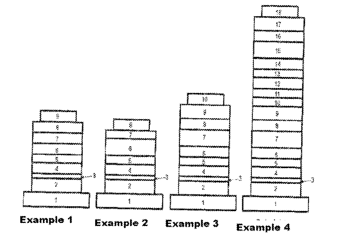
[0115]A sample on glass (1), silicon (2) as the gate electrode, oxidised silicon (3) as the dielectric with two gold electrodes as the source (4) and drain (5) and of the semiconductor layer (6) made from compounds having formula type A-C.

[0116]The following exemplary components were produced on the basis of the layer constructs shown in FIG. 9b.

example 1

Pin-Structure—Single Layers

[0117]A sample on glass (1), with trans-parent cover contact ITO (2), a relatively very thin layer of gold (3), a doped layer of PV-TPD (4), a relatively thin undoped layer of PV-TPD (5), a photoactive layer of compounds of formula type A-C (6), a photoactive layer of buckminsterfullerene C60 (7), an n-doped layer of C60 (8) and a cover contact of aluminium (9).

example 2

Pin-Structure—Mixed Layer

[0118]A sample on glass (1), with transparent cover contact ITO (2), a relatively very thin layer of gold (3), a doped layer of PV-TPD (4), a relatively thin undoped layer of PV-TPD (5), a photoactive mixed layer of C60 and compounds of formula type A-C (6), an n-doped layer of C60 (7), and a cover contact of aluminium (8).


PUM


Abstract

The present invention relates to an organic semiconductor element that comprises multiple layers. One or more layers may include compounds that can function as light absorbers, charge transporting materials, and / or as a dopant.

Description

FIELD OF THE INVENTION[0001]The present invention relates to a semiconductor element comprising multiple layers. One or more layers may also include compounds that may function as light absorbers, charge transporting material and / or a dopant.BACKGROUND OF THE INVENTION[0002]In recent years, organic compounds with high absorption capabilities in the red and infrared spectral range have generated considerable interest because of their suitability for use in many fields of science and technology. For example, compounds of such kind can be used as active media in laser-driven recordable media such as CD or DVDs, or in solar cells to convert thermal radiation into electrical energy and in thermal insulation materials to prevent the interiors of closed spaces from overheating, in motor vehicles or display window areas for example. At the same time, compounds of such kind that absorb long-wave energy must also have the properties of absorbing practically no energy in the shorter-wave, visi...

Claims


Application Information

Patent Timeline
IPC IPC(8): H01L51/30
CPCH01L51/0067H01L51/008Y02E10/549H01L51/42C09B55/003H01L51/0092H10K85/654H10K85/322H10K85/381H10K30/50H10K30/00
Inventor GRESSER, ROLANDMUELLER, TONIHUMMERT, MARKUSRIEDE, MORITZHARTMANN, HORSTLEO, KARL
Owner BASF AG
Learn More