Microfiber supported metal silicide nanowires

a technology of metal silicide and nanowires, which is applied in the manufacture of cables/conductors, chemical vapor deposition coatings, crystal growth processes, etc., can solve the problems of unsuitable methods, nanowires that cannot be reliably, precisely and precisely manufactured, and the nanowires that cannot be made by the same technique or tungsten silicide-based nanowires on the microfiber support have not been developed. , to achieve the effect of favorable characteristics of nanowir

Active Publication Date: 2012-09-27
UNIV OF WESTERN ONTARIO +1
View PDF1 Cites 20 Cited by
  • Summary
  • Abstract
  • Description
  • Claims
  • Application Information

AI Technical Summary

Benefits of technology

[0006]An arrangement of elongated nanowires that include titanium silicide or tungsten silicide may be grown on the exterior surfaces of many individual electrically conductive microfibers of much larger diameter. The relatively small nanowires are uniformly anchored along the exterior surfaces of the electrically conductive microfibers and, as such, protrude outwardly in all directions around the circumference of the microfibers to provide a wealth of flexible surface extensions. The final length and diameter dimensions of the surface-grown nanowires are substantially the same although they may grow at different rates. The titanium silicide or tungsten silicide contained in the nanowires imparts very favorable characteristics to the nanowires including electrically conductivity, thermally stability, and oxidation and corrosion resistance.

Problems solved by technology

But the techniques used to make these various nanowires have not been able to reliably, controllably, and precisely fabricate the nanowires in a way that makes their incorporation into electronic devices and electrochemical cells a viable option.
But, like the other nanowire forms, a suitable method that can produce a relatively dense quantity of spatially arranged titanium silicide- or tungsten silicide-based nanowires on a microfiber support has not previously been developed.

Method used


Image

  • Microfiber supported metal silicide nanowires
  • Microfiber supported metal silicide nanowires
  • Microfiber supported metal silicide nanowires

Examples


example

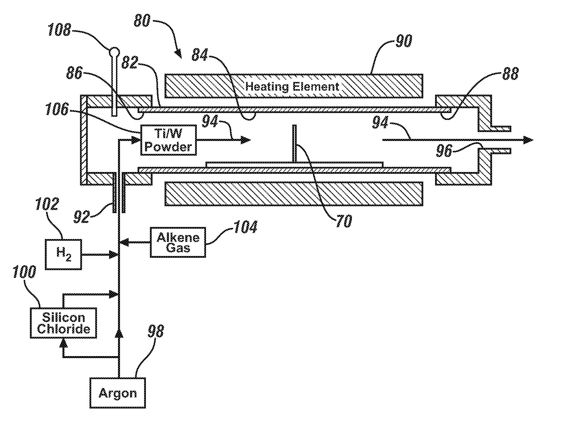
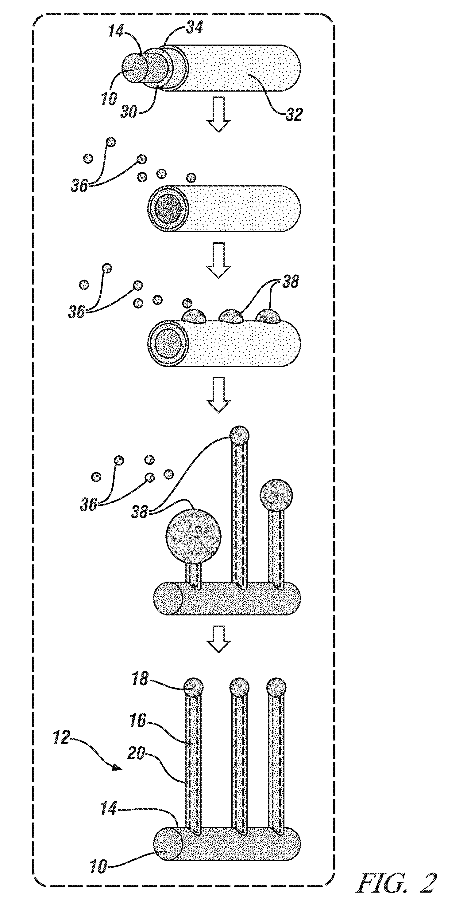
[0058]This example describes a specific process by which an arrangement of titanium silicide-based nanowires was grown on the surfaces of many individual carbon microfibers. Tungsten-based silicide nanowires could have been grown by simply depositing tungsten on the exterior surfaces of the carbon microfibers instead of titanium during the magnetron sputtering portion of the process. The same general observations and data trends that are discussed below for the titanium-silicide base nanowires would also be expected for the tungsten-based silicide nanowires.

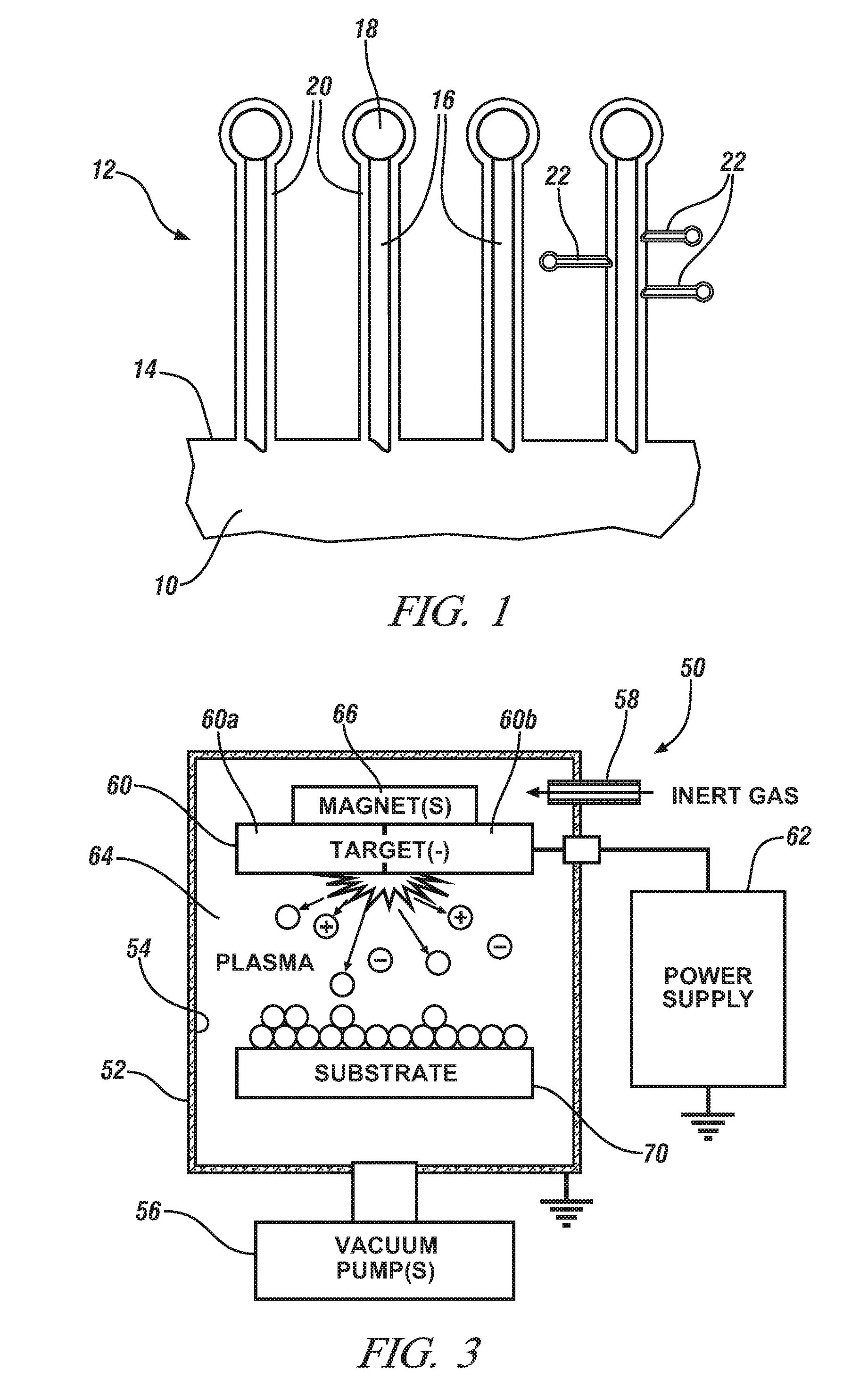
[0059]A commercially-available carbon paper comprised of a large quantity of carbon microfibers measuring 5 μm to 10 μm in diameter was obtained from E-TEK, a division of De Nora North America (Somerset, N.J.). A thin-film layer of pure titanium was deposited onto the surfaces of the carbon microfibers to a thickness of about 1 μm. The deposition of the titanium layer was accomplished by radio frequency (RF mode) magnetron sputte...


PUM

PropertyMeasurementUnit
thicknessaaaaaaaaaa
thicknessaaaaaaaaaa
temperatureaaaaaaaaaa

Abstract

An arrangement of elongated nanowires that include titanium silicide or tungsten silicide may be grown on the exterior surfaces of many individual electrically conductive microfibers of much larger diameter. Each of the nanowires is structurally defined by an elongated, centralized titanium silicide or tungsten silicide nanocore that terminates in a distally spaced gold particle and which is co-axially surrounded by a removable amorphous nanoshell. A gold-directed catalytic growth mechanism initiated during a low pressure chemical vapor deposition process is used to grow the nanowires uniformly along the entire length and circumference of the electrically conductive microfibers where growth is intended. The titanium silicide- or tungsten silicide-based nanowires can be used in a variety electrical, electrochemical, and semiconductor applications.

Description

TECHNICAL FIELD[0001]The technical field of this disclosure relates generally to microfiber-supported nanowires that include titanium silicide or tungsten silicide. Each of the nanowires is structurally defined by an elongated, centralized titanium silicide or tungsten silicide nanocore that terminates in a distally spaced gold particle and which is co-axially surrounded by a removable amorphous nanoshell. A gold-directed catalytic growth mechanism initiated during a low pressure chemical vapor deposition process is used to grow the nanowires uniformly along the entire length and circumference of many individual electrically conductive microfibers where growth is intended. Several physical properties of the nanowires can be selectively influenced by one or more controllable operating parameters associated with their growth.BACKGROUND[0002]Transition metal silicides are a class of semiconductor refractory materials. They are most commonly used by the microelectronics industry to fabr...

Claims


Application Information

Patent Timeline
Patent Type & Authority Applications(United States)
IPC IPC(8): H01B5/00C23C16/42H01B13/00C23C14/16B05D5/12C23C16/44B82Y40/00B82Y99/00
CPCB82Y30/00C30B29/10C04B35/62272C04B35/62857C04B35/62876C04B35/62894C04B35/62897C04B2235/46C04B2235/5248C04B2235/5256C04B2235/526C04B2235/5264C30B11/12C30B29/60B82Y40/00
Inventor CAI, MEISUN, XUELIANGZHANG, YONGBANIS, MOHAMMAD NOROUZILI, RUYING
Owner UNIV OF WESTERN ONTARIO
Why Eureka
Try Eureka