They tend to be precious, often due to their rarity in the Earth's crust.
As a result, when juxtaposed with a positive index material, negative index materials exhibit counterintuitive properties, like bending, or refracting, light in unnatural ways.
The time
delay between the two pulses is an additional degree of freedom, which gives strong interference effect in the SPP generation and propagation.
Thus, some types of optical resonances featured in one embodiment are
surface plasmon resonance, which results in anomalous reflection and high evanescent fields at
resonance.
Both approaches are based on the fabrication of permanent nanostructures on the
metal surface, which are very difficult if not impossible to reconfigure in real time.
Upon aggregation, the
plasmon resonances became severely damped, resulting in a blue color and eventually
precipitation of the
colloid.
Thermal therapies are simple and minimally invasive relative to conventional surgical treatments, although their effectiveness is limited by the ability to locally and specifically apply heat so as not to destroy
healthy tissue.
Upon
pulsed laser excitation, these clusters form
microbubbles owing to rapid heating at their surface, locally destroying the target cells thermolytically.
Generally, optical devices are difficult to miniaturize because photons can't be confined to areas much smaller than half their
wavelength.
For example, some require elaborate cooling systems and cannot operate at
room temperature, while some recent prior art overcomes this cooling limitation.
Optical data transfer, as in
fiber optics, allows
high bandwidth, but requires bulky “wires,” or tubes with reflective interiors.
The main limitation to plasmonics today in computing is that plasmons tend to dissipate after only a few millimeters, making them too short-lived to serve as a basis for computer chips, which are a few centimeters across.
Such rays can send avalanches of electrons streaming through delicate electronic components.
At best, this corrupts data and halts calculations.
At worst, it dramatically overheats transistors, permanently disabling them.
As the transistors in chips become smaller, the wires that connect them over distances of just a few nanometers become a significant
bottleneck for data.
Currently, such wires limit the speed at which electrons can deliver information, and an obvious solution is to replace them with photonic connections.
The problem with such connections to date has been converting electronic signals into photonic ones and back again with a speed and efficiency that makes it worthwhile.
With respect to the prior art, a major drawback of
semiconductor-based plasmonic elements and or
hybrid electrical-optical
chip systems is they typically involve a “top down”
assembly approach, and employ some form of
lithography and replication.
Top down approaches can be
time consuming, expensive and wasteful of materials.
Deposition of a
coating onto a
gold surface is not straightforward, and requires a clear understanding of the double layer properties of the material being coated, since the deposition must of necessity destroy the existing stabilizing layer of ions, charges or molecules at the surface.
With respect to plasmonic elements using nanometer scale pumping sources, such as LED's,
quantum dots, and the like, these sources are currently not considered suitable for
in vivo applications.
These nanoscale excitation sources can be functionalized onto one or more invention bio-
nanoparticle elements that also transport the plasmonic elements and their associated one or more types of
electromagnetic radiation and energy.iv) Another current plasmonic limitation is that a silica shell,
liposome,
micelle, and the like, by their inherent physical properties, typically comprise just one element containing a single plasmonic element, significantly limiting plasmonic configurations and functionalization flexibility.
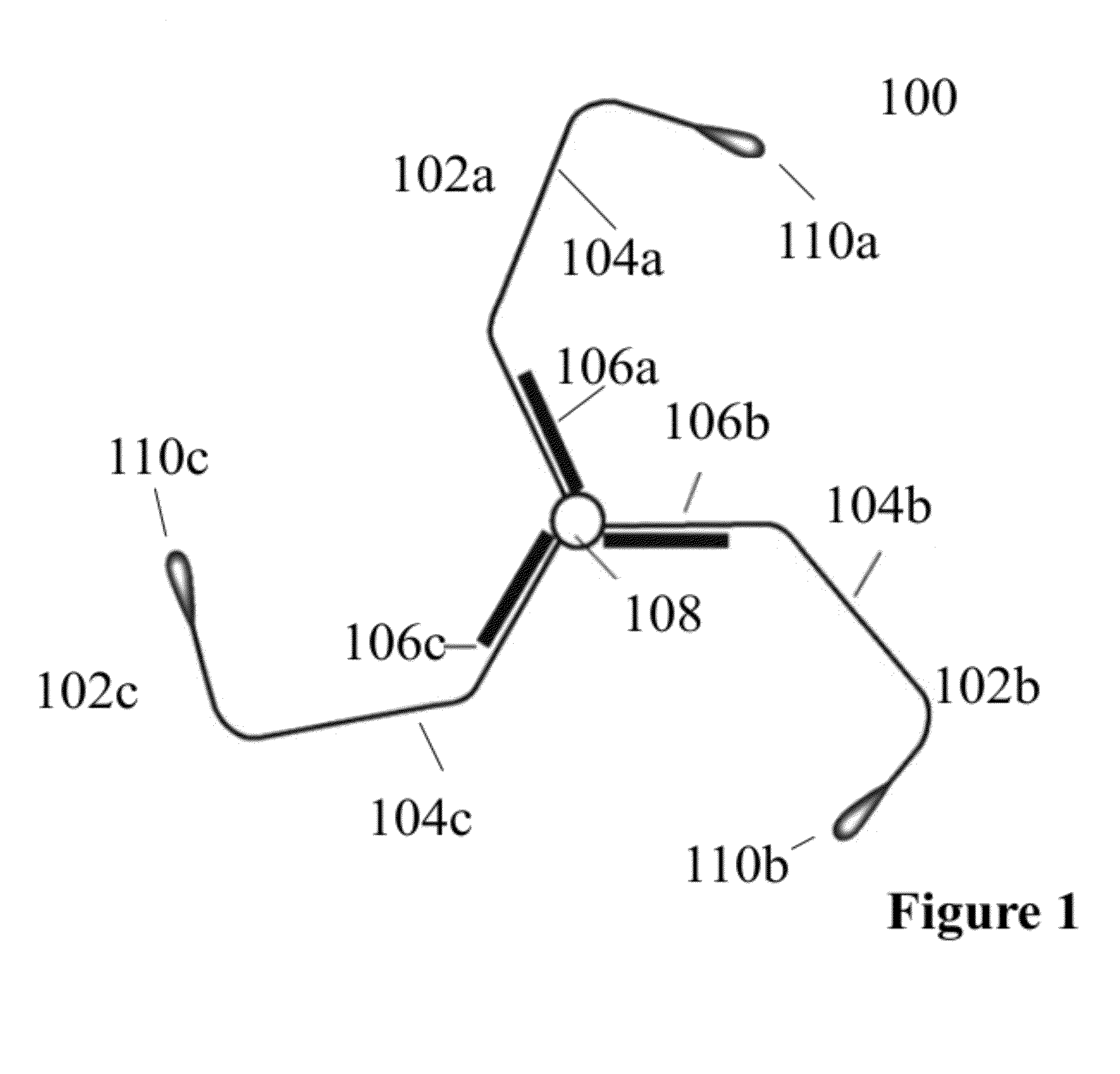
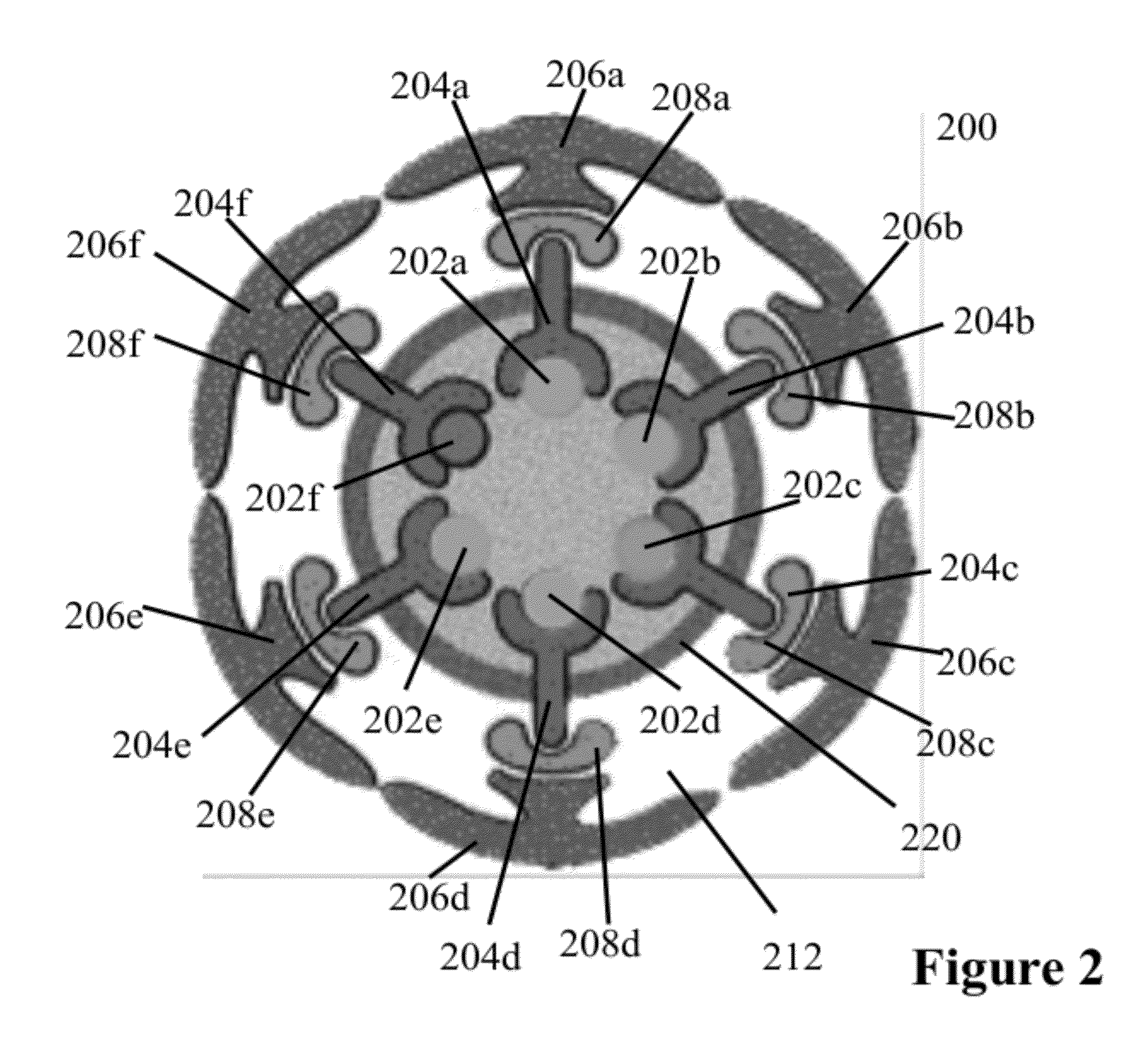
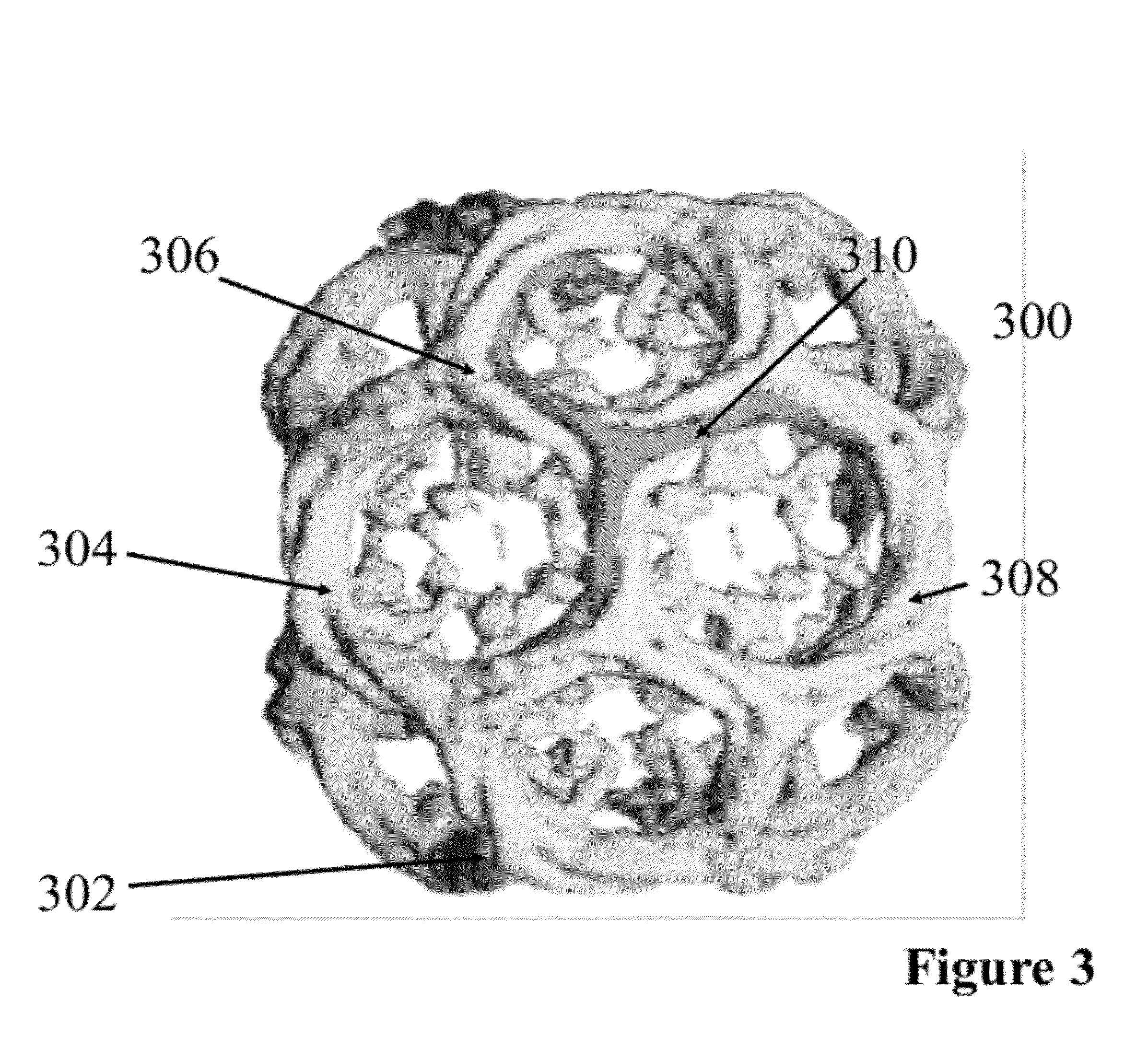
Instead, in one embodiment, one or more appropriately configured, metal coated, layered, and or structured metal coated surfaces comprising one or more clathrin and or coatomer partial protein cage elements of one or more types, like
monomer elements, and of one or more molecular weights are used.vi) Also, the physical properties of plasmonic elements like
semiconductor-based and silica shell elements, but not limited to, limit their applicability for
in vivo therapeutic and diagnostic applications in humans and animals, as there are the issues to overcome of tissue rejection,
toxicity, adverse reactions, renal clearance, and the like.

