Optical phase device, method and system.

Inactive Publication Date: 2013-05-09
BEIHANG UNIV
View PDF7 Cites 8 Cited by
  • Summary
  • Abstract
  • Description
  • Claims
  • Application Information

AI Technical Summary

Problems solved by technology

Although the existing technology can greatly enhanced the order of magnitude of the Goos-Hanchen shift from the wavelength level to the micron and even sub-millimeter level by designing the structure, which makes it practically usable, the enhancement of the phase variation corresponds to the enhanced absorption dip in the reflection spectrum, which is unavoidable in existing structure.
This leads to a very weak reflected intensity and a very low signal-to-noise ratio in the Goos-Hanchen shift detection, which increases the difficulty of detection and reduces the reliability of measurement.
But since its dispersion is so small that 1 km DCF can only compensate for the dispersion of 8 km-10 km normal single mode fiber.
Besides, the DCF has high transmission loss in the 1550 nm wavelength, and the

Method used


Image

  • Optical phase device, method and system.
  • Optical phase device, method and system.
  • Optical phase device, method and system.

Examples


example 2

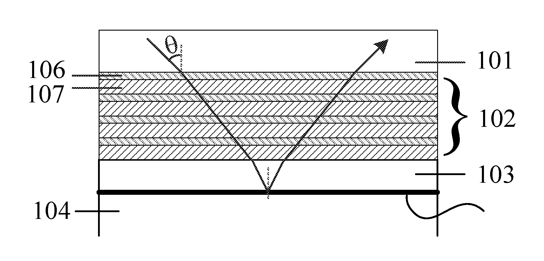
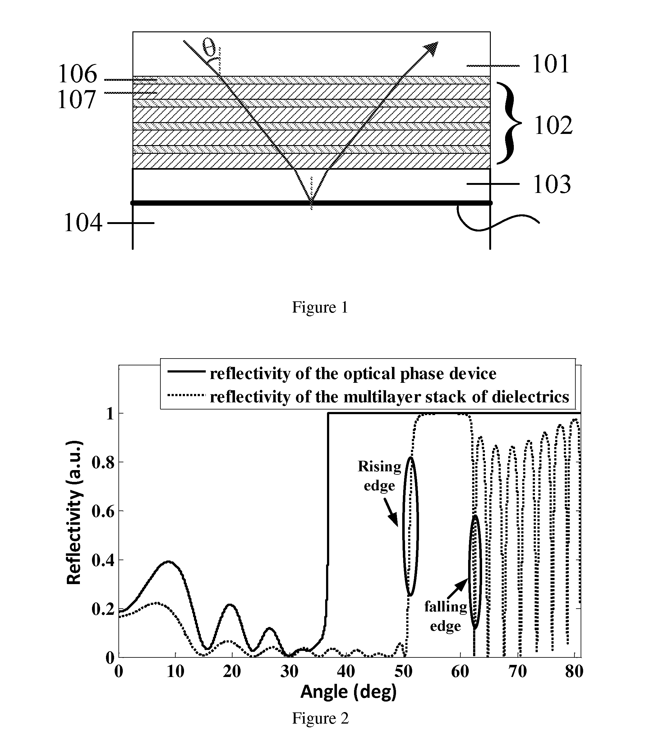
[0073]In this example, the polarization of the input light is TM polarization, and the wavelength is set as 980 nm. For the optical device structure shown in FIG. 1, the material of the transparent dielectric substrate 101 is ZF10 glass whose refractive index is 1.668; for the multilayer stack of dielectrics, the high refractive index dielectric thin layer 106 and the low refractive index dielectric thin layer 107 are arranged alternatively for 10 periods, wherein the material of the high refractive index dielectric thin layer 106 is titanium dioxide with refractive index of 2.3 and thickness as 196.7 nm; the material of the low refractive index dielectric thin layer 107 is silica with refractive index of 1.434 and thickness as 365.3 nm; the material of the buffer layer 103 is titanium dioxide with refractive index of 2.3 and thickness as 20 nm.

[0074]The optical phase device described above is used for Goos-Hanchen sensing detection, and the test sample is NaCl aqueous solutions of ...

example 3

[0097]The schematic diagram of the optical phase device used in this embodiment is as shown in FIG. 1. The material of the transparent dielectric substrate 101 is ZF1 glass. The multilayer stack of dielectrics 102 consists of 14 periods, and for each period, the high refractive index dielectric thin layer 106 is a layer of tantalum oxide with thickness of 264 nm and the low refractive index dielectric thin layer 107 is a 184 nm thick layer of silica. The buffer layer 103 is a layer of tantalum oxide of 21 nm thick, and the external medium 104 is air. The working range of the wavelength is 760-790 nm and the refractive index of each layer described above can be calculated through Sellmeier equation. By designing the thickness of each layer, high reflectivity region of this optical phase device can be designed.

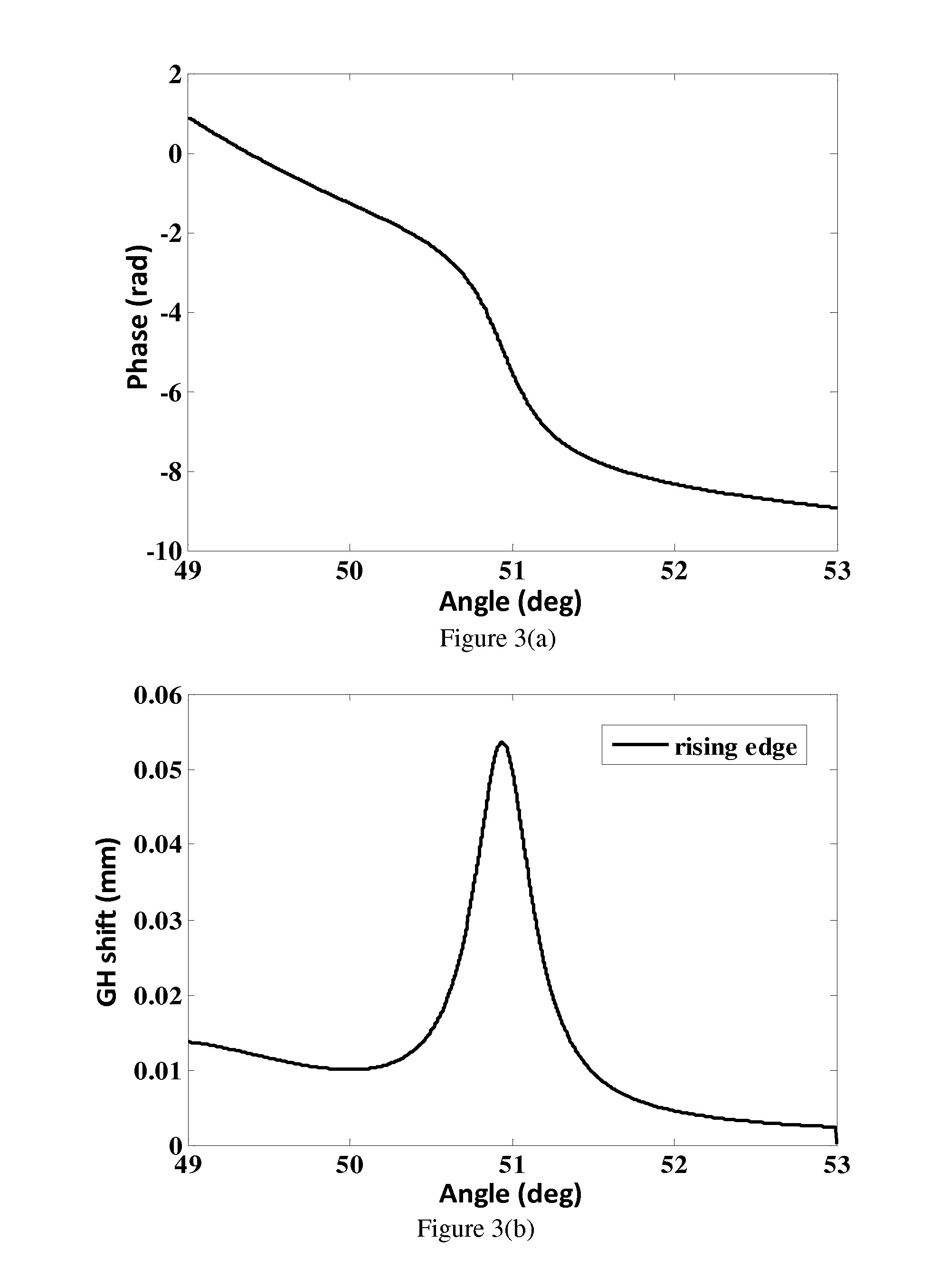
[0098]When the incident angle is 60 degree, the curve of the phase variation Δφ of multi-layer dielectric 102 against the wavelength λ, of the incident beam for TM polarization ...

example 4

[0104]In the device structure shown in FIG. 1, the incident wavelength is chosen as 980 nm. The material of the transparent dielectric substrate 101 is ZF10 glass, whose refractive index is 1.668. The multilayer stack of dielectrics 102 is composed of 10 periods, in which the high refractive index thin layer 106 is a layer of titanium dioxide whose refractive index is 2.3, and thickness is 163 nm, the low refractive index thin layer 107 is a layer of silica whose refractive index is 1.434 and thickness is 391 nm. The buffer layer 103 is a 23 nm thick titanium dioxide layer, whose refractive index is 2.3. FIG. 7 (a) shows the schematic diagram of the experimental setup for Goos-Hanchen shift measurement and sensing detection. In this embodiment, the polarization control device 702 is realized by a Glan prism and a half-wave plate, and the beam control device 703 is realized by a group of lenses and a pinhole. The waist of the output quasi-paralleled monochromatic beam is 750 microns....


PUM


Abstract

The invention provides an optical phase device, method and system. The optical phase device consists of a transparent dielectric substrate, a multilayer stack of dielectrics and a buffer layer. The refractive index of the transparent dielectric substrate, the multilayer stack of dielectrics and the buffer layer are all larger than that of the external medium. For the wavelength of the incident beam, the optical phase device has a phase variation in the angular range [α, β] and the critical angle for total reflection on the interface between the buffer layer and the external medium adjacent to the buffer layer is γ, γ<β. The optical device has both low loss and large phase variation, which leads to a large Goos-Hanchen shift. As a dispersion compensation component, it can produce larger, tunable dispersions, and different dispersion compensations can be obtained by adjusting the operating angle or parameters in the structure.

Description

PRIORITY CLAIM[0001]This application is a national phase application of and claims priority to PCT Patent Application No. PCT / CN2011 / 001705 published as WO2012159238, titled “OPTICAL PHASE DEVICE AS WELL AS APPLICATION METHOD AND SYSTEM THEREOF” by Zheng Zheng et al., filed Oct. 12, 2011, which claims priority to Chinese application No. 20110132978.X filed May 20, 2011, the specification and drawings of which are both herein expressly incorporated by reference in their entireties.FIELD OF THE INVENTION[0002]This invention involves sensing technology and dispersion compensation technology, especially involving an optical phase device with its application method and system.BACKGROUND OF THE INVENTION[0003]When the beam is reflected on the interface of which the refractivity is (including intensity and phase) not constant, a number of non-specular reflection phenomenon may happen. For example, there may exist a certain lateral displacement between the incident point and the emergent po...

Claims


Application Information

Patent Timeline
IPC IPC(8): G02B5/30
CPCG02B5/3083G02B27/283G02B5/0833G01N21/552
Inventor ZHENG, ZHENGWAN, YUHANGZHAO, XINLU, ZHITINGGUAN, JINGYI
Owner BEIHANG UNIV
Why Eureka
Try Eureka