

Switchable gas cluster and atomic ion gun, and method of surface processing using the gun
- Summary
- Abstract
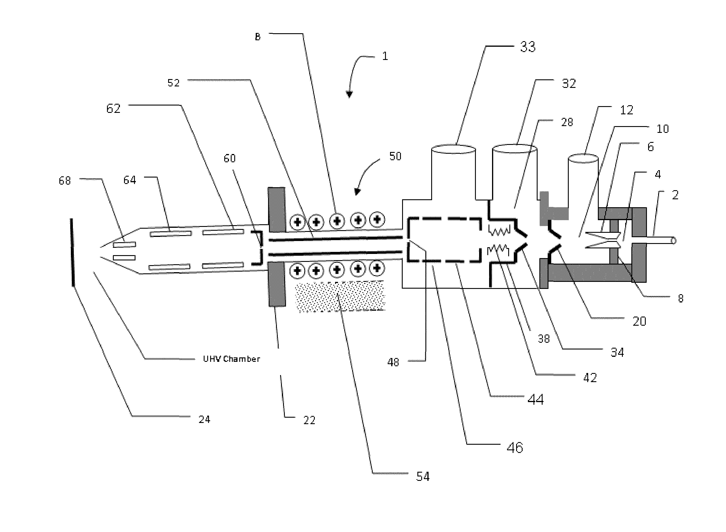
- Description
- Claims
- Application Information
AI Technical Summary
Benefits of technology
Problems solved by technology
Method used
Image

Examples
example 1
[0117]To illustrate its effectiveness, data was obtained from using the ion gun according to the invention to etch a PTFE polymer sample “as received” which had an XPS spectrum showing the C—F2 fluorocarbon bonds of the sample together with a layer of “adventitious carbon” contamination on the surface as shown in FIG. 5A. Attempts to remove this surface contamination with a conventional argon ion beam (200 eV) caused chemical damage to the sample as shown in FIG. 5B. However, when etching the surface with the ion gun according to the invention in cluster mode (source energy 4 key; minimum cluster size=200 atoms; max energy per atom=20 eV) etching with a cluster beam resulted in a clean undamaged spectrum as shown in FIG. 5C.
example 2
[0118]Referring to FIG. 6 there are shown XPS results on a silicon wafer having initially a thin film of Silicon Oxide thereon. FIG. 6A shows the Si 2p XPS scan from the wafer before etching, i.e. at etch time=0 s and etch level=0. The etch level is an arbitrary unit related to the depth of etching, which can be translated into a true “depth” once the etch rate is determined by using a calibrated sample. In the scan of un-etched wafer separate peaks can be seen for the pure un-oxidised silicon (large peak) and the silicon oxide (small peak). The ion gun was then set to its argon atomic ion mode and argon ions as ionised single argon atoms at a source energy of 4 keV irradiated the surface of the wafer to depth profile through the silicon oxide surface film. As shown in FIG. 6B at an etch level of 178, the XPS spectrum of the wafer after the depth profiling was completed shows only the un-oxidised silicon. The XPS depth profile in FIG. 6C shows the gradual removal of the adventitious...
example 3
[0119]Referring to FIG. 7 there are shown XPS results for depth profiling on another very delicate sample, a fluoropolymer film on a PTFE substrate using the ion gun in its cluster mode with the same settings as Example 1. It is well known that PTFE is easily damaged by ion beam bombardment. As shown in FIG. 7A, before etching, and during the depth profile, a well resolved fluoropolymer spectrum is observed showing the details of the sample chemistry. After etching through the film, a spectrum as shown in FIG. 7B of the undamaged PTFE substrate is observed showing only the C—F2 bonded carbon of PTFE, with no peaks corresponding to any broken C—F or C—C bonds. The depth profile shown in FIG. 7C shows the transition through an undamaged fluoropolymer film into an undamaged PTFE film.
PUM
| Property | Measurement | Unit |
|---|---|---|
| Angle | aaaaa | aaaaa |
| Angle | aaaaa | aaaaa |
| Diameter | aaaaa | aaaaa |
Abstract
Description
Claims
Application Information