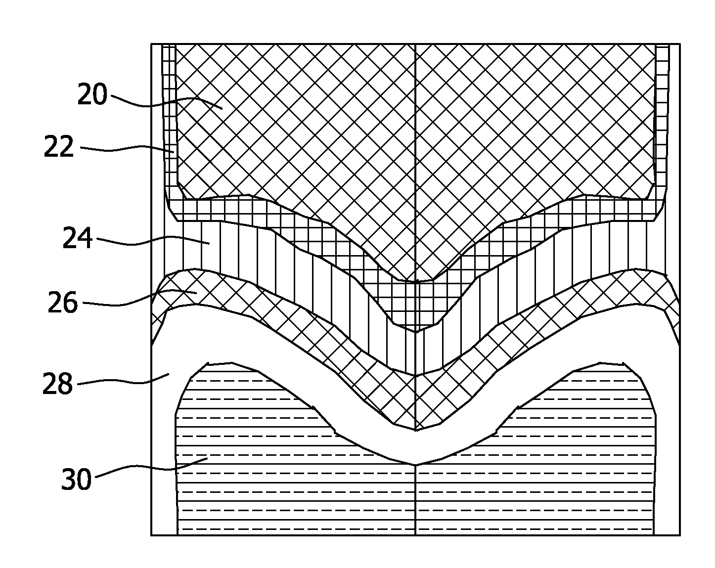
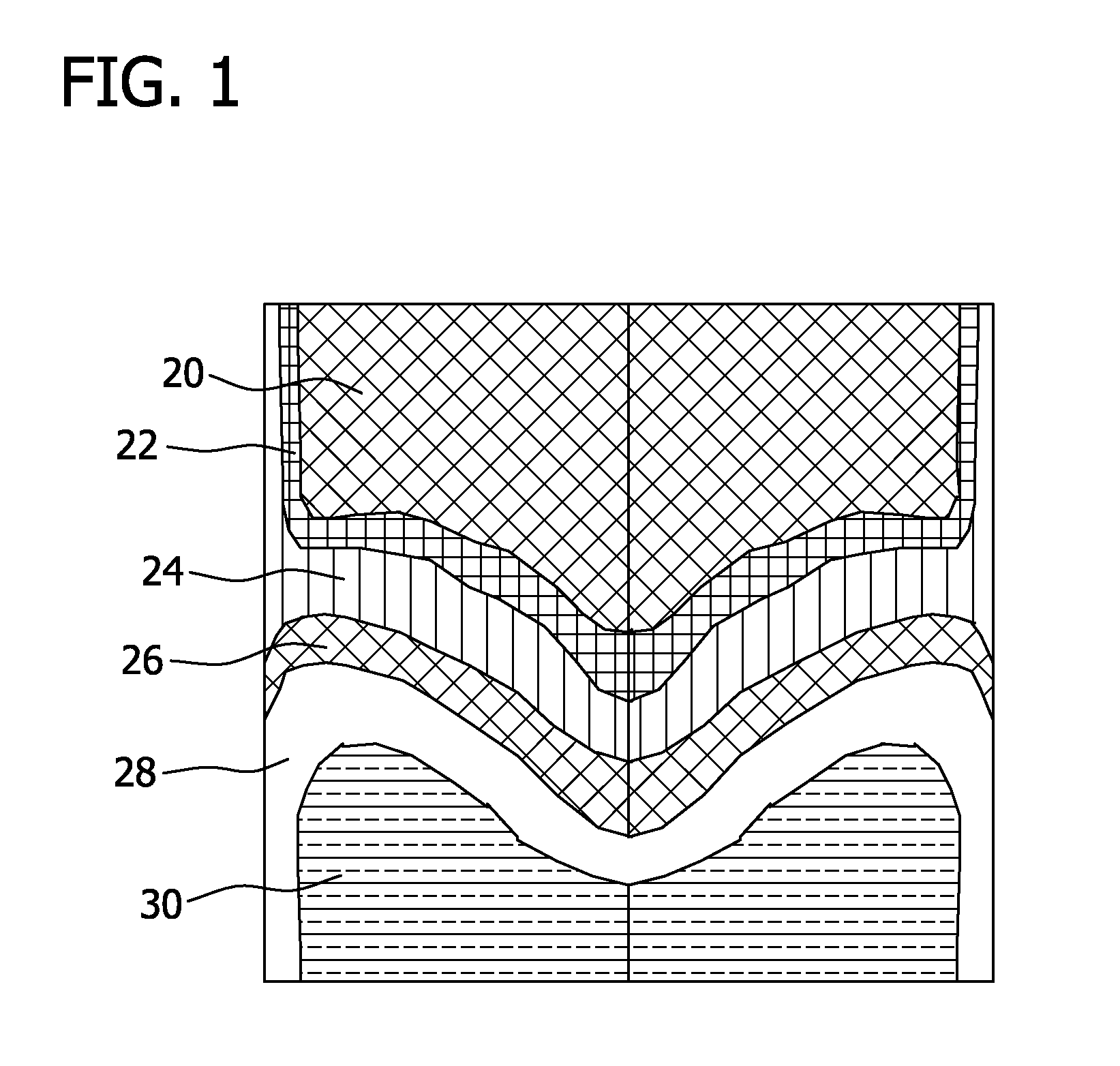
Qualitative crystal defect evaluation method
- Summary
- Abstract
- Description
- Claims
- Application Information
AI Technical Summary
Benefits of technology
Problems solved by technology
Method used
Image

Examples
example 1
Copper Decoration of Silicon Wafer
[0046]Copper decoration was carried out on a silicon wafer sample. The silicon wafer sample was etched and polished according to conventional techniques. A saturated solution of copper nitrate (Cu(NO3)4.5H2O) was spread in a thin film on the back of the sample. The sample was heated to between 50° C. and 60° C. on a hot plate to dry the solution. The sample was annealed for 5 to 20 minutes per sample thickness at 900° C. in muffle furnace and air-quenched to room temperature. The anneal duration was dependent upon the sample thickness. Thinner wafers required a shorter anneal, while thicker wafers required a longer anneal.
[0047]The sample was etched to a mirror finished using mixed acid etchant mixture (57% Nitric Acid (70%), 18% Hydrofluoric Acid (49%) and 25% Hydrochloric Acid), followed by Secco Etch (0.15M Potassium Dichromate and 49% Hydrofluoric Acid, 1:2 ratio). After rinsing and drying, the sample was visually inspected under bright or room ...
example 3
Copper Decoration of Annealed Silicon Wafer
[0050]An etched and polished sample was loaded into a boat and placed in a tube furnace preheated to between 500° C. and 700° C. with 1 slpm oxygen gas environment. The sample was heated to 1100° C. with faster than 7° C. / min ramping speed. The sample holding time at high temperature was 10 min in 2 slpm oxygen gas environment. The sample was cooled down faster than 7° C. / min to a temperature lower than 500° C.
[0051]A saturated solution of copper nitrate (Cu(NO3)4.5H2O) was spread in a thin film on the back of the sample. The sample was heated to between 50° C. and 60° C. on a hot plate to dry the solution. The sample was annealed for 5 to 20 minutes per sample thickness at 900° C. in muffle furnace and air-quenched to room temperature. The anneal temperature was dependent upon the sample thickness. Thinner wafers required a shorter anneal, while thicker wafers required a longer anneal.
[0052]The sample was etched to a mirror finished using ...
example 4
Copper Decoration of Annealed Silicon Wafer
[0053]An etched and polished sample was loaded into a boat and placed in a tube furnace pre-heated to between 500° C. and 700° C. with 1 slpm oxygen gas environment. The sample was heated to 1200° C. with faster than 7° C. / min ramping speed. The sample holding time at high temperature was 10 min in 2slpm oxygen gas environment. The sample was cooled down faster than 7° C. / min to a temperature lower than 500° C.
[0054]A saturated solution of copper nitrate (Cu(NO3)4.5H2O) was spread in a thin film on the back of the sample. The sample was heated to between 50° C. and 60° C. on a hot plate to dry the solution. The sample was annealed for 5 to 20 minutes per sample thickness at 900° C. in muffle furnace and air-quenched to room temperature. The anneal temperature was dependent upon the sample thickness. Thinner wafers required a shorter anneal, while thicker wafers required a longer anneal.
[0055]The sample was etched to a mirror finished using ...
PUM
| Property | Measurement | Unit |
|---|---|---|
| Temperature | aaaaa | aaaaa |
| Temperature | aaaaa | aaaaa |
| Temperature | aaaaa | aaaaa |
Abstract
Description
Claims
Application Information
 - R&D
- Intellectual Property
- Life Sciences
- Materials
- Tech Scout
- Unparalleled Data Quality
- Higher Quality Content
- 60% Fewer Hallucinations
Browse by: Latest US Patents, China's latest patents, Technical Efficacy Thesaurus, Application Domain, Technology Topic, Popular Technical Reports.
© 2025 PatSnap. All rights reserved.Legal|Privacy policy|Modern Slavery Act Transparency Statement|Sitemap|About US| Contact US: help@patsnap.com