
Method for producing an organic semiconductor device

a semiconductor device and organic technology, applied in semiconductor devices, solid-state devices, thermoelectric devices, etc., can solve the problems of reducing the efficiency of semiconductor devices, affecting the performance of semiconductor devices, etc., to achieve the effect of suppressing the ambipolar charge carrier transpor

Active Publication Date: 2013-08-08
CLAP CO LTD
View PDF3 Cites 15 Cited by
  • Summary
  • Abstract
  • Description
  • Claims
  • Application Information

AI Technical Summary

Benefits of technology

The patent text discusses a new type of organic semiconducting material that can be used to make electronic devices. This material is made up of naphthalene-based semiconducting polymers that have high carrier mobility and good current modulation characteristics. These polymers can also be solution-processable and stable in air. They can be used to make p-type or n-type semiconductor materials, which in turn can be used to make various electronics devices. The use of an intermediate layer, called a self-assembled monolayer, is also discussed, which can help with the fabrication process. Overall, the patent text describes a way to make organic semiconductor devices with improved performance using advanced materials and processes.

Problems solved by technology

This ambipolar region, however, leads to several technical challenges.
Further, secondly, complex effects of trapping of charge carriers occur, since one or both types of charge carriers are subject to different trapping, specifically due to their different chemical properties, such as different chemical moieties.
Hence, a pronounced ambipolarity in many cases is undesirable, such as for applications such as display backplanes utilizing OTFTs.
Besides the technical challenges regarding the design of materials and charge transport, electrode design has known to be a key issue in improving the performance of organic electronic devices.
Thus, in organic field effect transistors, while moving into smaller channel length regions to provide higher performance, contact resistance has become a more prominent problem.
Thus, in many cases, the contact resistance issue has come forward due to the mismatch in energy level between the work function of the metal electrode and the HOMO of the organic semiconducting material (for hole injection) and / or due to the mismatch in energy level between the work function of the metal electrode and the LUMO of the organic semiconducting material (for electron injection).
It is known that SAMs on metal electrodes may affect the work function of the electrode.
However, as outlined above, ambipolarity of organic transistor devices in many technical applications is unwanted and leads to technical challenges.
Specifically, control of transistor devices having ambipolar charge carrier transport is rather difficult.
Specifically, mainly due to the chemical stability of negative charges in organic materials, the design of n-type organic semiconducting materials and, thereby, the design of n-channel organic field effect transistors still remains an open issue.

Method used


Image

  • Method for producing an organic semiconductor device
  • Method for producing an organic semiconductor device
  • Method for producing an organic semiconductor device

Examples


example 1

Polymer Synthesis

[0221]The following examples describe the preparation of certain polymers of the present teachings and related intermediates.

example 1a

Preparation of poly{[N,N′-bis(2-ethylhexyl)-1,4,5,8-naphthalene diimide-2,6-diyl]-alt-5,5′-(2,2′-bithiophene)} [P(NDI2EH-T2)]

Preparation of 2,6-dibromonaphthalene-1,4,5,8-tetracarboxydianhydride (NDA-Br2)

[0222]A mixture of 1,4,5,8-naphthalenetetracarboxylic dianhydride (2.8 g, 10.3 mmol) and oleum (20% SO3, 100 mL) was stirred at 55° C. for 2 hours. To this mixture, a solution of dibromoisocyanuric acid (3.0 g, 10.5 mmol) in oleum (50 mL) was added over 40 mins. The resulting mixture was then warmed to 85° C. and maintained at this temperature for 43 hours. After cooling to room temperature, the reaction mixture was poured onto crushed ice (420 g), diluted with water (400 mL), and then stirred at room temperature for 1 hour. The resulting precipitates were collected by centrifugation, washed with water and methanol, collected by centrifugation and finally dried under vacuum, leading to a greenish yellow solid (3.6 g, 8.5 mmol, yield 82.2%). Elemental Analysis (calc. C, 39.47; H, 0.4...

example 1b

Preparation of poly{[N,N′-bis(2-ethylhexyl)-1,4,5,8-naphthalene diimide-2,6-diyl]-alt-2,5-thiophene} [P(NDI2EH-T1)]

Preparation of Copolymer P(NDI2EH-T1)

[0227]Under argon, a mixture of NDI2EH-Br2 (Example 1A, 84 mg, 0.13 mmol), 2,5-bis(trimethylstannyl)thiophene (53 mg, 0.13 mmol), and Pd(PPh3)2Cl2 (3.0 mg, 0.004 mmol) in anhydrous toluene (5 mL) was stirred at 90° C. for 4 days. Bromobenzene (0.3 mL) was then added and the resulting mixture was stirred at 90° C. for an additional 12 hours. Upon cooling to room temperature, a solution of potassium fluoride (1.2 g) in water (2.5 mL) was added. This mixture was stirred at room temperature for 2 hours and the precipitate collected by filtration. The solid was taken with a small amount of chloroform, methanol was added, and the resulting solid collected by filtration. This procedure was repeated using chloroform and acetone, leading to a deep blue solid as the crude product (20.0 mg, yield 20.7%). Elemental Analysis (calc. C, 71.55; H, 6...


PUM

PropertyMeasurementUnit
channel lengthaaaaaaaaaa
conductivityaaaaaaaaaa

Abstract

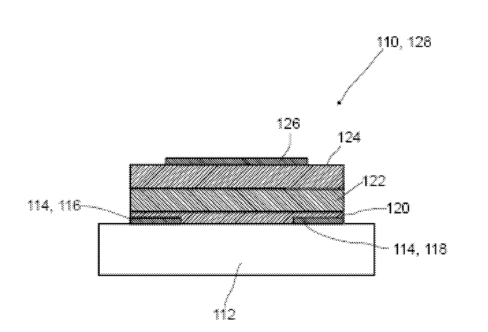
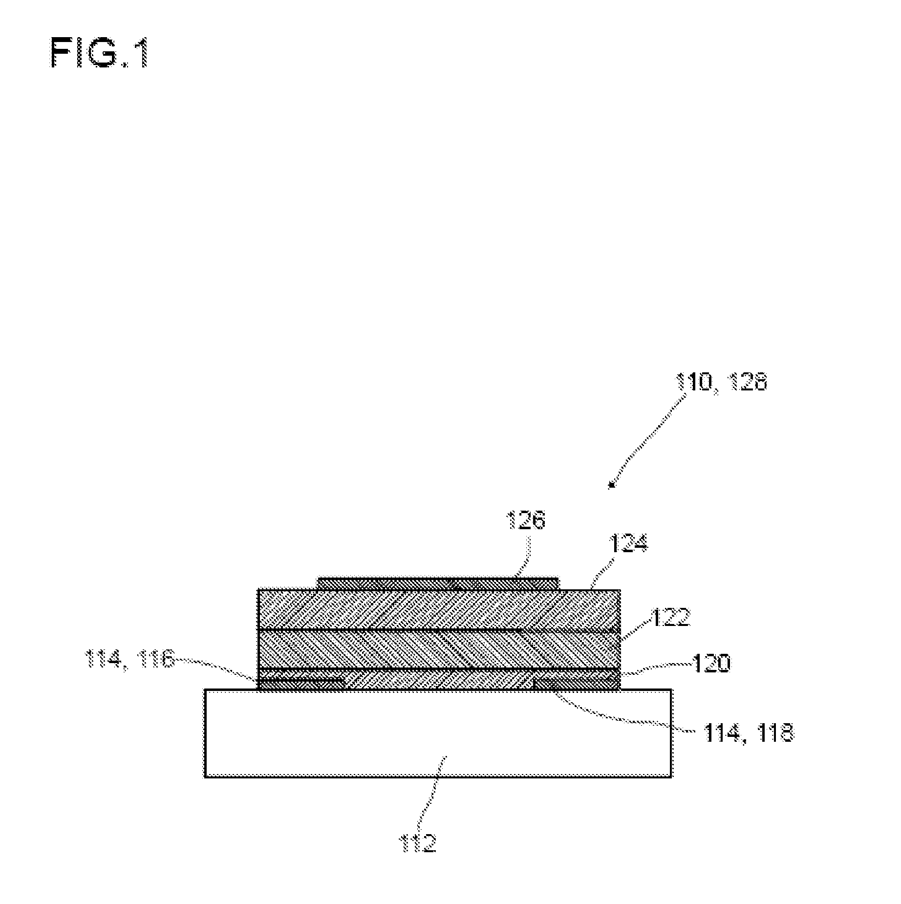
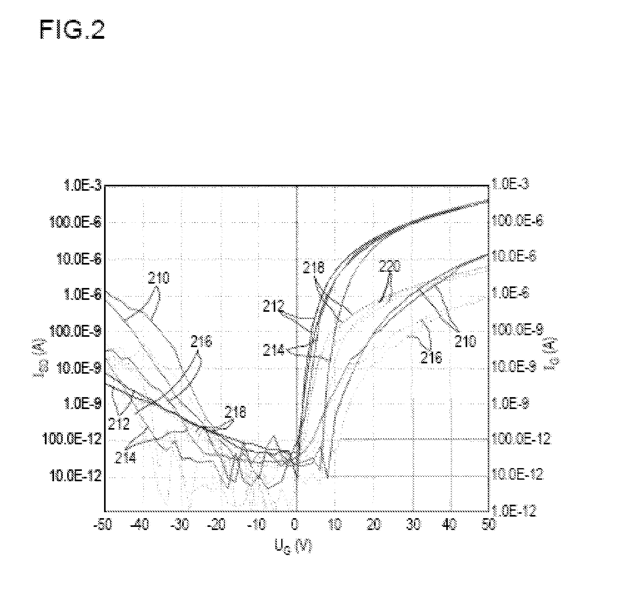
A method for producing an organic semiconductor device (110) having at least one organic semiconducting material (122) and at least two electrodes (114) adapted to support an electric charge carrier transport through the organic semiconducting material (122) is disclosed. The organic semiconducting material (122) intrinsically has ambipolar semiconducting properties. The method comprises at least one step of generating at least one intermediate layer (120) which at least partially is interposed between the organic semiconducting material (122) and at least one of the electrodes (114) of the organic semiconductor device (110). The intermediate layer (120) comprises at least one thiol compound having the general formula HS—R, wherein R is an organic residue. The thiol compound has an electric dipole moment pointing away from the SH-group of the thiol compound. The electric dipole moment has at least the same magnitude as the electric dipole moment in 4-Phenylthiophenol. By the intermediate layer (120) an ambipolar charge carrier transport between the electrodes (114) is suppressed in favor of a unipolar charge carrier transport.

Description

FIELD OF THE INVENTION[0001]The invention relates to a method for producing an organic semiconductor device. In further aspects, the invention relates to an organic semiconductor device and to a use of an intermediate layer comprising at least one thiol compound for suppressing an ambipolar charge carrier transport in favor of a unipolar charge carrier transport in an organic semiconductor device. The method, the organic semiconductor device and the use according to the present invention preferably may be applied in the field of organic electronics in general or, more preferably, in the field of organic field effect transistors (OFETs).RELATED ART[0002]In recent years, organic semiconductors, such as polymeric semiconductors, monomeric semiconductors or oligomeric semiconductors, have received considerable attention as promising alternative materials to conventional semiconductors, such as silicon. Thus, in various fields of electronics, conventional, inorganic semiconducting materi...

Claims


Application Information

Patent Timeline
Patent Type & Authority Applications(United States)
IPC IPC(8): H01L51/30H01L51/40
CPCC08G2261/124H01L51/0558C08G2261/146C08G2261/312C08G2261/3223C08G2261/3229C08G2261/3246C08G2261/3327C08G2261/334C08G2261/344C08G2261/364C08G2261/414C08G2261/51C08G2261/92C08G61/126H01L51/0036H01L51/0043C08G2261/1412H10K85/113H10K85/151H10K10/484
Inventor VAIDYANATHAN, SUBRAMANIANKASTLER, MARCELTAN, BERTHAZHOU, MI
Owner CLAP CO LTD
Learn More